MCP1640EV-SBC Microchip Technology, MCP1640EV-SBC Datasheet - Page 11
MCP1640EV-SBC
Manufacturer Part Number
MCP1640EV-SBC
Description
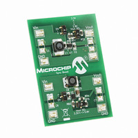
BOARD EVAL FOR MCP1640
Manufacturer
Microchip Technology
Type
DC/DC Switching Converters, Regulators & Controllersr
Datasheets
1.MCP1640CT-ICHY.pdf
(32 pages)
2.MCP1640CT-ICHY.pdf
(26 pages)
3.MCP1640EV-SBC.pdf
(22 pages)
Specifications of MCP1640EV-SBC
Main Purpose
DC/DC, Step Up
Outputs And Type
1, Non-Isolated
Voltage - Output
2V, 3.3V or 5V
Current - Output
100mA, 350mA
Voltage - Input
0.35 ~ 5.5V
Regulator Topology
Boost
Frequency - Switching
500kHz
Board Type
Fully Populated
Utilized Ic / Part
MCP1640
Input Voltage
0.35 V to 5.5 V
Output Voltage
3.3 V to 5 V
Operating Supply Voltage
0.35 V to 5.5 V
Product
Power Management Modules
Supply Current
300 mA
Kit Contents
Board
Features
Automatic PFM/PWM Operation, Enable State Selectable Using Mini-Dip Switch On Board
Svhc
No SVHC (15-Dec-2010)
Core Architecture
Power Management - Voltage Regulator
Rohs Compliant
Yes
For Use With/related Products
MCP1640
Lead Free Status / RoHS Status
Contains lead / RoHS non-compliant
Power - Output
-
Lead Free Status / Rohs Status
Lead free / RoHS Compliant
Available stocks
Company
Part Number
Manufacturer
Quantity
Price
Company:

Part Number:
MCP1640EV-SBC
Manufacturer:
Microchip Technology
Quantity:
135
Company:
Part Number:
MCP1640EV-SBC
Manufacturer:
MICROCHIP
Quantity:
12 000


4.0
4.1
The MCP1640/B/C/D family of devices is capable of
low start-up voltage and delivers high efficiency over a
wide load range for single cell, two cell, three cell
alkaline, NiMH, NiCd and single cell Li-Ion battery
inputs. A high level of integration lowers total system
cost, eases implementation and reduces board area.
The devices feature low start-up voltage, adjustable
output voltage, PWM/PFM mode operation, low I
integrated synchronous switch, internal compensation,
low noise anti-ring control, inrush current limit and soft
start. There are two feature options for the MCP1640/
B/C/D family: PWM/PFM mode or PWM mode only,
and “true output disconnect” or input bypass.
4.1.1
The MCP1640/C devices use an automatic switchover
from PWM to PFM mode for light load conditions to
maximize efficiency over a wide range of output
current. During PFM mode, higher peak current is used
to pump the output up to the threshold limit. While
operating in PFM or PWM mode, the P-Channel switch
is used as a synchronous rectifier, turning off when the
inductor current reaches 0 mA to maximize efficiency.
In PFM mode, a comparator is used to terminate
switching when the output voltage reaches the upper
threshold limit. Once switching has terminated, the
output voltage will decay or coast down. During this
period, very low I
input source, which keeps power efficiency high at light
load. The disadvantages of PWM/PFM mode are
higher output ripple voltage and variable PFM mode
frequency. The PFM mode frequency is a function of
input voltage, output voltage and load. While in PFM
mode, the boost converter pumps the output up at a
switching frequency of 500 kHz.
4.1.2
The MCP1640B/D devices disable PFM mode
switching, and operate only in PWM mode over the
entire load range. During periods of light load opera-
tion, the MCP1640B/D continues to operate at a con-
stant 500 kHz switching frequency keeping the output
ripple voltage lower than PFM mode. During PWM only
mode, the MCP1640B/D P-Channel switch acts as a
synchronous rectifier by turning off to prevent reverse
current flow from the output cap back to the input in
order to keep efficiency high. For noise immunity, the
N-Channel MOSFET current sense is blanked for
approximately 100 ns. With a typical minimum duty
cycle of 100 ns, the MCP1640B/D continues to switch
at a constant frequency under light load conditions.
Figure 2-12
current for the pulse skipping threshold in PWM only
mode. At lighter loads, the MCP1640B/D devices begin
to skip pulses.
2010 Microchip Technology Inc.
DETAILED DESCRIPTION
Device Option Overview
PWM/PFM MODE OPTION
PWM MODE ONLY OPTION
represents the input voltage versus load
Q
is consumed from the device and
Q
,
4.1.3
The MCP1640/B devices incorporate a true output
disconnect feature. With the EN pin pulled low, the
output of the MCP1640/B is isolated or disconnected
from the input by turning off the integrated P-Channel
switch and removing the switch bulk diode connection.
This removes the DC path typical in boost converters,
which allows the output to be disconnected from the
input. During this mode, less than 1 µA of current is
consumed from the input (battery). True output discon-
nect does not discharge the output; the output voltage
is held up by the external C
4.1.4
The MCP1640C/D devices incorporate the input
bypass shutdown option. With the EN input pulled low,
the output is connected to the input using the internal
P-Channel MOSFET. In this mode, the current draw
from the input (battery) is less than 1 µA with no load.
The Input Bypass mode is used when the input voltage
range is high enough for the load to operate in Sleep or
low I
necessary to operate the application, the EN input is
pulled high enabling the boost converter.
TABLE 4-1:
MCP1640
MCP1640B
MCP1640C
MCP1640D
Number
Q
Part
mode. When a higher regulated output voltage is
TRUE OUTPUT DISCONNECT
OPTION
INPUT BYPASS OPTION
MCP1640/B/C/D
PWM/
PFM
PART NUMBER SELECTION
X
X
PWM
OUT
X
X
capacitance.
True Dis Bypass
DS22234A-page 11
X
X
X
X
Related parts for MCP1640EV-SBC
Image
Part Number
Description
Manufacturer
Datasheet
Request
R

Part Number:
Description:
0.65V Start-up Synchronous Boost Regulator with True Output Disconnect or Input/Output Bypass Option
Manufacturer:
MICROCHIP [Microchip Technology]
Datasheet:

Part Number:
Description:
IC CONV DC-DC STEPUP SYNC 8DFN
Manufacturer:
Microchip Technology
Datasheet:

Part Number:
Description:
0.65v Start-up Synchronous Boost Regulator With True Output Disconnect Or Input/output Bypass Option
Manufacturer:
Microchip Technology Inc.
Datasheet:
Part Number:
Description:
Manufacturer:
Microchip Technology Inc.
Datasheet:
Part Number:
Description:
Manufacturer:
Microchip Technology Inc.
Datasheet:
Part Number:
Description:
Manufacturer:
Microchip Technology Inc.
Datasheet:
Part Number:
Description:
Manufacturer:
Microchip Technology Inc.
Datasheet:
Part Number:
Description:
Manufacturer:
Microchip Technology Inc.
Datasheet:
Part Number:
Description:
Manufacturer:
Microchip Technology Inc.
Datasheet:
Part Number:
Description:
Manufacturer:
Microchip Technology Inc.
Datasheet: