MCP1640EV-SBC Microchip Technology, MCP1640EV-SBC Datasheet - Page 4
MCP1640EV-SBC
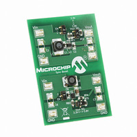
Manufacturer Part Number
MCP1640EV-SBC
Description
BOARD EVAL FOR MCP1640
Manufacturer
Microchip Technology
Type
DC/DC Switching Converters, Regulators & Controllersr
Datasheets
1.MCP1640CT-ICHY.pdf
(32 pages)
2.MCP1640CT-ICHY.pdf
(26 pages)
3.MCP1640EV-SBC.pdf
(22 pages)
Specifications of MCP1640EV-SBC
Main Purpose
DC/DC, Step Up
Outputs And Type
1, Non-Isolated
Voltage - Output
2V, 3.3V or 5V
Current - Output
100mA, 350mA
Voltage - Input
0.35 ~ 5.5V
Regulator Topology
Boost
Frequency - Switching
500kHz
Board Type
Fully Populated
Utilized Ic / Part
MCP1640
Input Voltage
0.35 V to 5.5 V
Output Voltage
3.3 V to 5 V
Operating Supply Voltage
0.35 V to 5.5 V
Product
Power Management Modules
Supply Current
300 mA
Kit Contents
Board
Features
Automatic PFM/PWM Operation, Enable State Selectable Using Mini-Dip Switch On Board
Svhc
No SVHC (15-Dec-2010)
Core Architecture
Power Management - Voltage Regulator
Rohs Compliant
Yes
For Use With/related Products
MCP1640
Lead Free Status / RoHS Status
Contains lead / RoHS non-compliant
Power - Output
-
Lead Free Status / Rohs Status
Lead free / RoHS Compliant
Available stocks
Company
Part Number
Manufacturer
Quantity
Price
Company:

Part Number:
MCP1640EV-SBC
Manufacturer:
Microchip Technology
Quantity:
135
Company:
Part Number:
MCP1640EV-SBC
Manufacturer:
MICROCHIP
Quantity:
12 000


MCP1640/B/C/D
DC CHARACTERISTICS (CONTINUED)
TEMPERATURE SPECIFICATIONS
DS22234A-page 4
Electrical Characteristics: Unless otherwise indicated, V
T
Boldface specifications apply over the T
NMOS Peak Switch Current
Limit
V
Line Regulation
Load Regulation
Maximum Duty Cycle
Switching Frequency
EN Input Logic High
EN Input Logic Low
EN Input Leakage Current
Soft-start Time
Thermal Shutdown Die
Temperature
Die Temperature Hysteresis
Note 1:
Electrical Specifications:
Temperature Ranges
Operating Junction Temperature
Range
Storage Temperature Range
Maximum Junction Temperature
Package Thermal Resistances
Thermal Resistance, 5L-TSOT23
Thermal Resistance, 8L-2x3 DFN
A
OUT
= +25°C.
Accuracy
2:
3:
4:
5:
Parameters
3.3 K resistive load, 3.3V
For V
I
estimated by: (I
220 resistive load, 3.3V
Peak current limit determined by characterization, not production tested.
Parameters
Q
is measured from V
IN
> V
OUT
, V
QPFM
OUT
* (V
will not remain in regulation.
OUT
V
V
T
V
V
DC
I
V
N(MAX)
I
V
Sym
SDHYS
A
OUT
OUT
OUT
OUT
ENLK
T
f
V
; V
OUT
V
t
SW
OUT
SS
OUT
range of -40
SD
MAX
OUT
IH
Sym
IL
IN
T
IN
T
T
/V
%
) /
JA
JA
|
(15 mA).
A
|
J
J
/
/
(1 mA).
quiescent current will vary with boost ratio. V
IN
)), (I
Min
600
425
88
90
—
—
—
—
—
-3
-1
-1
QPWM
Min
o
-40
-65
—
—
—
C to +85
IN
= 1.2V, C
* (V
0.005
o
0.01
0.01
Typ
850
500
750
150
C.
Typ
192
90
10
OUT
—
—
—
93
—
—
—
/V
OUT
IN
)).
= C
+125
+150
+150
Max
Max
IN
575
—
—
+3
20
—
—
—
—
—
—
—
1
1
= 10 µF, L = 4.7 µH, V
%of V
%of V
Units
°C/W
°C/W
Units
°C
°C
°C
%/V
kHz
mA
µA
µS
C
C
%
%
%
IN
IN
Steady State
Transient
EIA/JESD51-3 Standard
IN
2010 Microchip Technology Inc.
Note 5
Includes Line and Load
Regulation; V
V
I
I
V
I
I
V
EN Low to High, 90% of
V
OUT
OUT
OUT
OUT
quiescent current can be
IN
IN
EN
OUT
OUT
= 1.5V to 3V
= 1.5V
= 5V
= 25 mA
= 25 mA to 100 mA;
= 1 mA
= 1 mA
; Note 4
= 3.3V, I
Conditions
Conditions
IN
OUT
= 1.5V
= 15 mA,
Related parts for MCP1640EV-SBC
Image
Part Number
Description
Manufacturer
Datasheet
Request
R

Part Number:
Description:
0.65V Start-up Synchronous Boost Regulator with True Output Disconnect or Input/Output Bypass Option
Manufacturer:
MICROCHIP [Microchip Technology]
Datasheet:

Part Number:
Description:
IC CONV DC-DC STEPUP SYNC 8DFN
Manufacturer:
Microchip Technology
Datasheet:

Part Number:
Description:
0.65v Start-up Synchronous Boost Regulator With True Output Disconnect Or Input/output Bypass Option
Manufacturer:
Microchip Technology Inc.
Datasheet:
Part Number:
Description:
Manufacturer:
Microchip Technology Inc.
Datasheet:
Part Number:
Description:
Manufacturer:
Microchip Technology Inc.
Datasheet:
Part Number:
Description:
Manufacturer:
Microchip Technology Inc.
Datasheet:
Part Number:
Description:
Manufacturer:
Microchip Technology Inc.
Datasheet:
Part Number:
Description:
Manufacturer:
Microchip Technology Inc.
Datasheet:
Part Number:
Description:
Manufacturer:
Microchip Technology Inc.
Datasheet:
Part Number:
Description:
Manufacturer:
Microchip Technology Inc.
Datasheet: