MCP1640EV-SBC Microchip Technology, MCP1640EV-SBC Datasheet - Page 9
MCP1640EV-SBC
Manufacturer Part Number
MCP1640EV-SBC
Description
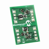
BOARD EVAL FOR MCP1640
Manufacturer
Microchip Technology
Type
DC/DC Switching Converters, Regulators & Controllersr
Datasheets
1.MCP1640CT-ICHY.pdf
(32 pages)
2.MCP1640CT-ICHY.pdf
(26 pages)
3.MCP1640EV-SBC.pdf
(22 pages)
Specifications of MCP1640EV-SBC
Main Purpose
DC/DC, Step Up
Outputs And Type
1, Non-Isolated
Voltage - Output
2V, 3.3V or 5V
Current - Output
100mA, 350mA
Voltage - Input
0.35 ~ 5.5V
Regulator Topology
Boost
Frequency - Switching
500kHz
Board Type
Fully Populated
Utilized Ic / Part
MCP1640
Input Voltage
0.35 V to 5.5 V
Output Voltage
3.3 V to 5 V
Operating Supply Voltage
0.35 V to 5.5 V
Product
Power Management Modules
Supply Current
300 mA
Kit Contents
Board
Features
Automatic PFM/PWM Operation, Enable State Selectable Using Mini-Dip Switch On Board
Svhc
No SVHC (15-Dec-2010)
Core Architecture
Power Management - Voltage Regulator
Rohs Compliant
Yes
For Use With/related Products
MCP1640
Lead Free Status / RoHS Status
Contains lead / RoHS non-compliant
Power - Output
-
Lead Free Status / Rohs Status
Lead free / RoHS Compliant
Available stocks
Company
Part Number
Manufacturer
Quantity
Price
Company:

Part Number:
MCP1640EV-SBC
Manufacturer:
Microchip Technology
Quantity:
135
Company:
Part Number:
MCP1640EV-SBC
Manufacturer:
MICROCHIP
Quantity:
12 000


3.0
The descriptions of the pins are listed in
TABLE 3-1:
3.1
Connect the inductor from the input voltage to the SW
pin. The SW pin carries inductor current and can be as
high as 800 mA peak. The integrated N-Channel switch
drain and integrated P-Channel switch source are inter-
nally connected at the SW node.
3.2
The ground or return pin is used for circuit ground con-
nection. Length of trace from input cap return, output
cap return and GND pin should be made as short as
possible to minimize noise on the GND pin. In the
SOT23-6 package, a single ground pin is used.
3.3
The EN pin is a logic-level input used to enable or
disable device switching and lower quiescent current
while disabled. A logic high (>90% of V
the regulator output. A logic low (<20% of V
ensure that the regulator is disabled.
3.4
The FB pin is used to provide output voltage regulation
by using a resistor divider. The FB voltage will be 1.21V
typical with the output voltage in regulation.
3.5
The output voltage pin connects the integrated
P-Channel MOSFET to the output capacitor. The FB
voltage divider is also connected to the V
voltage regulation.
2010 Microchip Technology Inc.
SW
GND
EN
FB
V
V
S
P
V
V
EP
Pin No.
OUT
IN
GND
GND
OUTS
OUTP
PIN DESCRIPTIONS
Switch Node Pin (SW)
Ground Pin (GND)
Enable Pin (EN)
Feedback Voltage Pin (FB)
Output Voltage Pin (V
MCP1640/B/C/D
SOT23
PIN FUNCTION TABLE
—
1
2
3
4
5
6
MCP1640/B/C/D
2x3 DFN
OUT
5
4
1
8
2
3
7
6
9
IN
Table
)
) will enable
OUT
3-1.
IN
pin for
Switch Node, Boost Inductor Input Pin
Ground Pin
Enable Control Input Pin
Feedback Voltage Pin
Output Voltage Pin
Input Voltage Pin
Signal Ground Pin
Power Ground Pin
Output Voltage Sense Pin
Output Voltage Power Pin
Exposed Thermal Pad (EP); must be connected to V
) will
3.6
Connect the input voltage source to V
source should be decoupled to GND with a 4.7 µF
minimum capacitor.
3.7
The signal ground pin is used as a return for the
integrated V
package, the S
connected externally.
3.8
The power ground pin is used as a return for the high-
current N-Channel switch. In the 2x3 DFN package, the
P
externally.
3.9
The output voltage sense pin connects the regulated
output voltage to the internal bias circuits. In the 2x3
DFN package, V
externally.
3.10
The output voltage power pin connects the output volt-
age to the switch node. High current flows through the
integrated P-Channel and out of this pin to the output
capacitor and output. In the 2x3 DFN package, V
and V
3.11
There is no internal electrical connection between the
Exposed Thermal Pad (EP) and the P
pins. They must be connected to the same potential on
the Printed Circuit Board (PCB).
GND
OUTP
and signal ground (S
Power Supply Input Voltage Pin
(V
Signal Ground Pin (S
Power Ground Pin (P
Output Voltage Sense Pin (V
Output Voltage Power Pin (V
Exposed Thermal Pad (EP)
are connected externally.
IN
REF
MCP1640/B/C/D
Description
)
GND
and error amplifier. In the 2x3 DFN
OUTS
and power ground (P
and V
GND
OUTP
) pins are connected
GND
GND
DS22234A-page 9
SS.
are connected
GND
IN
GND
)
)
. The input
and S
) pins are
OUTS
OUTP
OUTS
GND
)
)
Related parts for MCP1640EV-SBC
Image
Part Number
Description
Manufacturer
Datasheet
Request
R

Part Number:
Description:
0.65V Start-up Synchronous Boost Regulator with True Output Disconnect or Input/Output Bypass Option
Manufacturer:
MICROCHIP [Microchip Technology]
Datasheet:

Part Number:
Description:
IC CONV DC-DC STEPUP SYNC 8DFN
Manufacturer:
Microchip Technology
Datasheet:

Part Number:
Description:
0.65v Start-up Synchronous Boost Regulator With True Output Disconnect Or Input/output Bypass Option
Manufacturer:
Microchip Technology Inc.
Datasheet:
Part Number:
Description:
Manufacturer:
Microchip Technology Inc.
Datasheet:
Part Number:
Description:
Manufacturer:
Microchip Technology Inc.
Datasheet:
Part Number:
Description:
Manufacturer:
Microchip Technology Inc.
Datasheet:
Part Number:
Description:
Manufacturer:
Microchip Technology Inc.
Datasheet:
Part Number:
Description:
Manufacturer:
Microchip Technology Inc.
Datasheet:
Part Number:
Description:
Manufacturer:
Microchip Technology Inc.
Datasheet:
Part Number:
Description:
Manufacturer:
Microchip Technology Inc.
Datasheet: