MCP1640EV-SBC Microchip Technology, MCP1640EV-SBC Datasheet - Page 15
MCP1640EV-SBC
Manufacturer Part Number
MCP1640EV-SBC
Description
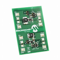
BOARD EVAL FOR MCP1640
Manufacturer
Microchip Technology
Type
DC/DC Switching Converters, Regulators & Controllersr
Datasheets
1.MCP1640CT-ICHY.pdf
(32 pages)
2.MCP1640CT-ICHY.pdf
(26 pages)
3.MCP1640EV-SBC.pdf
(22 pages)
Specifications of MCP1640EV-SBC
Main Purpose
DC/DC, Step Up
Outputs And Type
1, Non-Isolated
Voltage - Output
2V, 3.3V or 5V
Current - Output
100mA, 350mA
Voltage - Input
0.35 ~ 5.5V
Regulator Topology
Boost
Frequency - Switching
500kHz
Board Type
Fully Populated
Utilized Ic / Part
MCP1640
Input Voltage
0.35 V to 5.5 V
Output Voltage
3.3 V to 5 V
Operating Supply Voltage
0.35 V to 5.5 V
Product
Power Management Modules
Supply Current
300 mA
Kit Contents
Board
Features
Automatic PFM/PWM Operation, Enable State Selectable Using Mini-Dip Switch On Board
Svhc
No SVHC (15-Dec-2010)
Core Architecture
Power Management - Voltage Regulator
Rohs Compliant
Yes
For Use With/related Products
MCP1640
Lead Free Status / RoHS Status
Contains lead / RoHS non-compliant
Power - Output
-
Lead Free Status / Rohs Status
Lead free / RoHS Compliant
Available stocks
Company
Part Number
Manufacturer
Quantity
Price
Company:

Part Number:
MCP1640EV-SBC
Manufacturer:
Microchip Technology
Quantity:
135
Company:
Part Number:
MCP1640EV-SBC
Manufacturer:
MICROCHIP
Quantity:
12 000


5.0
5.1
The MCP1640/B/C/D synchronous boost regulator
operates over a wide input voltage and output voltage
range. The power efficiency is high for several decades
of load range. Output current capability increases with
input voltage and decreases with increasing output
voltage. The maximum output current is based on the
N-Channel peak current limit. Typical characterization
curves in this data sheet are presented to display the
typical output current capability.
5.2
To calculate the resistor divider values for the
MCP1640/B/C/D, the following equation can be used.
Where R
to GND and both are connected to the FB input pin.
EQUATION 5-1:
Example A:
V
V
R
R
Example B:
V
V
R
R
There are some potential issues with higher value
resistors.
environment contamination can create leakage paths
that significantly change the resistor divider that effect
the output voltage. The FB input leakage current can
also impact the divider and change the output voltage
tolerance.
2010 Microchip Technology Inc.
OUT
FB
OUT
FB
BOT
TOP
BOT
TOP
= 1.21V
= 1.21V
= 3.3V
= 309 k
= 533.7 k (Standard Value = 536 k)
= 5.0V
= 309 k
= 967.9 k (Standard Value = 976 k)
TOP
APPLICATION INFORMATION
Typical Applications
Adjustable Output Voltage
Calculations
R
TOP
For
is connected to V
=
small
R
BOT
surface
OUT
V
------------ - 1
V
OUT
, R
FB
mount
BOT
–
is connected
resistors,
5.3
The boost input current is smoothed by the boost
inductor reducing the amount of filtering necessary at
the input. Some capacitance is recommended to
provide decoupling from the source. Low ESR X5R or
X7R are well suited since they have a low temperature
coefficient and small size. For most applications,
4.7 µF of capacitance is sufficient at the input. For high
power applications that have high source impedance or
long leads, connecting the battery to the input 10 µF of
capacitance
capacitance can be added to provide a stable input
voltage.
Table 5-1
input capacitor value.
5.4
The output capacitor helps provide a stable output
voltage during sudden load transients and reduces the
output voltage ripple. As with the input capacitor, X5R
and X7R ceramic capacitors are well suited for this
application.
The MCP1640/B/C/D is internally compensated so
output capacitance range is limited. See
the recommended output capacitor range.
While the N-Channel switch is on, the output current is
supplied by the output capacitor C
output capacitance and equivalent series resistance
will have a significant effect on the output ripple
voltage. While C
drop also appears across its internal ESR that results
in ripple voltage.
EQUATION 5-2:
Where dV represents the ripple voltage and dt
represents the ON time of the N-Channel switch (D * 1/
F
Table 5-1
input and output capacitor value.
TABLE 5-1:
SW
).
Max
Min
Input Capacitor Selection
Output Capacitor Selection
contains the recommended range for the
contains the recommended range for the
MCP1640/B/C/D
I
OUT
is
OUT
CAPACITOR VALUE RANGE
recommended.
=
provides load current, a voltage
4.7 µF
C
none
C
OUT
IN
OUT
dV
------ -
dt
DS22234A-page 15
Additional
. The amount of
Table 5-1
100 µF
10 µF
C
OUT
input
for
Related parts for MCP1640EV-SBC
Image
Part Number
Description
Manufacturer
Datasheet
Request
R

Part Number:
Description:
0.65V Start-up Synchronous Boost Regulator with True Output Disconnect or Input/Output Bypass Option
Manufacturer:
MICROCHIP [Microchip Technology]
Datasheet:

Part Number:
Description:
IC CONV DC-DC STEPUP SYNC 8DFN
Manufacturer:
Microchip Technology
Datasheet:

Part Number:
Description:
0.65v Start-up Synchronous Boost Regulator With True Output Disconnect Or Input/output Bypass Option
Manufacturer:
Microchip Technology Inc.
Datasheet:
Part Number:
Description:
Manufacturer:
Microchip Technology Inc.
Datasheet:
Part Number:
Description:
Manufacturer:
Microchip Technology Inc.
Datasheet:
Part Number:
Description:
Manufacturer:
Microchip Technology Inc.
Datasheet:
Part Number:
Description:
Manufacturer:
Microchip Technology Inc.
Datasheet:
Part Number:
Description:
Manufacturer:
Microchip Technology Inc.
Datasheet:
Part Number:
Description:
Manufacturer:
Microchip Technology Inc.
Datasheet:
Part Number:
Description:
Manufacturer:
Microchip Technology Inc.
Datasheet: