MCP1640EV-SBC Microchip Technology, MCP1640EV-SBC Datasheet - Page 3
MCP1640EV-SBC
Manufacturer Part Number
MCP1640EV-SBC
Description
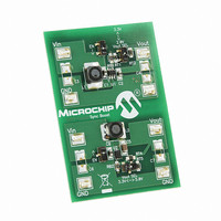
BOARD EVAL FOR MCP1640
Manufacturer
Microchip Technology
Type
DC/DC Switching Converters, Regulators & Controllersr
Datasheets
1.MCP1640CT-ICHY.pdf
(32 pages)
2.MCP1640CT-ICHY.pdf
(26 pages)
3.MCP1640EV-SBC.pdf
(22 pages)
Specifications of MCP1640EV-SBC
Main Purpose
DC/DC, Step Up
Outputs And Type
1, Non-Isolated
Voltage - Output
2V, 3.3V or 5V
Current - Output
100mA, 350mA
Voltage - Input
0.35 ~ 5.5V
Regulator Topology
Boost
Frequency - Switching
500kHz
Board Type
Fully Populated
Utilized Ic / Part
MCP1640
Input Voltage
0.35 V to 5.5 V
Output Voltage
3.3 V to 5 V
Operating Supply Voltage
0.35 V to 5.5 V
Product
Power Management Modules
Supply Current
300 mA
Kit Contents
Board
Features
Automatic PFM/PWM Operation, Enable State Selectable Using Mini-Dip Switch On Board
Svhc
No SVHC (15-Dec-2010)
Core Architecture
Power Management - Voltage Regulator
Rohs Compliant
Yes
For Use With/related Products
MCP1640
Lead Free Status / RoHS Status
Contains lead / RoHS non-compliant
Power - Output
-
Lead Free Status / Rohs Status
Lead free / RoHS Compliant
Available stocks
Company
Part Number
Manufacturer
Quantity
Price
Company:

Part Number:
MCP1640EV-SBC
Manufacturer:
Microchip Technology
Quantity:
135
Company:
Part Number:
MCP1640EV-SBC
Manufacturer:
MICROCHIP
Quantity:
12 000


1.0
Absolute Maximum Ratings †
EN, FB, V
EN, FB ...........<greater of V
Output Short Circuit Current....................... Continuous
Output Current Bypass Mode........................... 400 mA
Power Dissipation ............................ Internally Limited
Storage Temperature .........................-65
Ambient Temp. with Power Applied......-40
Operating Junction Temperature........-40
ESD Protection On All Pins:
DC CHARACTERISTICS
2010 Microchip Technology Inc.
Electrical Characteristics: Unless otherwise indicated, V
T
Boldface specifications apply over the T
Input Characteristics
Minimum Start-Up Voltage
Minimum Input Voltage After
Start-Up
Output Voltage Adjust Range
Maximum Output Current
Feedback Voltage
Feedback Input Bias Current
Quiescent Current – PFM
Mode
Quiescent Current – PWM
Mode
Quiescent Current – Shutdown
NMOS Switch Leakage
PMOS Switch Leakage
NMOS Switch ON Resistance
PMOS Switch ON Resistance
Note 1:
A
= +25°C.
2:
3:
4:
5:
ELECTRICAL
CHARACTERISTICS
HBM........................................................ 3 kV
MM........................................................ 300 V
IN,
Parameters
3.3 K resistive load, 3.3V
For V
I
estimated by: (I
220 resistive load, 3.3V
Peak current limit determined by characterization, not production tested.
Q
V
is measured from V
SW
IN
, V
> V
OUT
OUT
- GND ........................... +6.5V
, V
QPFM
OUT
OUT
or V
* (V
will not remain in regulation.
OUT
R
R
I
I
DS(ON)N
I
QSHDN
DS(ON)P
V
QPWM
A
Sym
QPFM
OUT
IN
I
OUT
I
I
I
V
V
V
OUT
; V
VFB
NLK
PLK
OUT
range of -40
OUT
FB
IN
IN
> (GND - 0.3V)
IN
/V
o
o
(15 mA).
C to +150
C to +125
o
(1 mA).
quiescent current will vary with boost ratio. V
IN
C to +85
)), (I
1.175
Min
100
2.0
—
—
—
—
—
—
—
—
—
—
QPWM
o
C to +85
o
o
o
IN
C
C
C
= 1.2V, C
* (V
o
0.65
0.35
1.21
0.05
Typ
150
150
350
220
0.7
0.3
0.6
0.9
C.
10
19
OUT
/V
OUT
† Notice: Stresses above those listed under “Maximum
Ratings” may cause permanent damage to the device.
This is a stress rating only and functional operation of
the device at those or any other conditions above those
indicated
specification is not intended. Exposure to maximum
rating conditions for extended periods may affect
device reliability.
IN
)).
= C
1.245
Max
IN
0.8
5.5
2.3
0.2
30
—
—
—
—
—
—
—
—
1
= 10 µF, L = 4.7 µH, V
in
MCP1640/B/C/D
the
Units
mA
mA
mA
µA
pA
µA
µA
µA
µA
V
V
V
V
operational
IN
Note 1
Note 1
V
1.2V V
1.5V V
3.3V V
—
—
Measured at V
EN = V
Note 3
Measured at V
I
V
Includes N-Channel and
P-Channel Switch Leakage
V
5.5V V
V
V
V
V
OUT
quiescent current can be
OUT
OUT
IN
IN
OUT
IN
IN
OUT
= V
= VS
= 3.3V, I
= 3.3V, I
= 0 mA; Note 3
= 5.5V
V
= EN = GND;
IN
IN
IN
EN
IN
SW
= 3.3V, I
Conditions
, 2.0V V
, 3.3V V
, 5.0V V
W
, I
IN
= V
sections
= 5V; V
OUT
= GND;
; Note 2
SW
SW
DS22234A-page 3
FB
OUT
OUT
OUT
= 0 mA;
= 100 mA
= 100 mA
= GND
OUT
OUT
OUT
; EN = V
OUT
= 15 mA,
= 4.0V;
of
=
this
IN
Related parts for MCP1640EV-SBC
Image
Part Number
Description
Manufacturer
Datasheet
Request
R

Part Number:
Description:
0.65V Start-up Synchronous Boost Regulator with True Output Disconnect or Input/Output Bypass Option
Manufacturer:
MICROCHIP [Microchip Technology]
Datasheet:

Part Number:
Description:
IC CONV DC-DC STEPUP SYNC 8DFN
Manufacturer:
Microchip Technology
Datasheet:

Part Number:
Description:
0.65v Start-up Synchronous Boost Regulator With True Output Disconnect Or Input/output Bypass Option
Manufacturer:
Microchip Technology Inc.
Datasheet:
Part Number:
Description:
Manufacturer:
Microchip Technology Inc.
Datasheet:
Part Number:
Description:
Manufacturer:
Microchip Technology Inc.
Datasheet:
Part Number:
Description:
Manufacturer:
Microchip Technology Inc.
Datasheet:
Part Number:
Description:
Manufacturer:
Microchip Technology Inc.
Datasheet:
Part Number:
Description:
Manufacturer:
Microchip Technology Inc.
Datasheet:
Part Number:
Description:
Manufacturer:
Microchip Technology Inc.
Datasheet:
Part Number:
Description:
Manufacturer:
Microchip Technology Inc.
Datasheet: