MCP1640EV-SBC Microchip Technology, MCP1640EV-SBC Datasheet - Page 16
MCP1640EV-SBC
Manufacturer Part Number
MCP1640EV-SBC
Description
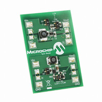
BOARD EVAL FOR MCP1640
Manufacturer
Microchip Technology
Type
DC/DC Switching Converters, Regulators & Controllersr
Datasheets
1.MCP1640CT-ICHY.pdf
(32 pages)
2.MCP1640CT-ICHY.pdf
(26 pages)
3.MCP1640EV-SBC.pdf
(22 pages)
Specifications of MCP1640EV-SBC
Main Purpose
DC/DC, Step Up
Outputs And Type
1, Non-Isolated
Voltage - Output
2V, 3.3V or 5V
Current - Output
100mA, 350mA
Voltage - Input
0.35 ~ 5.5V
Regulator Topology
Boost
Frequency - Switching
500kHz
Board Type
Fully Populated
Utilized Ic / Part
MCP1640
Input Voltage
0.35 V to 5.5 V
Output Voltage
3.3 V to 5 V
Operating Supply Voltage
0.35 V to 5.5 V
Product
Power Management Modules
Supply Current
300 mA
Kit Contents
Board
Features
Automatic PFM/PWM Operation, Enable State Selectable Using Mini-Dip Switch On Board
Svhc
No SVHC (15-Dec-2010)
Core Architecture
Power Management - Voltage Regulator
Rohs Compliant
Yes
For Use With/related Products
MCP1640
Lead Free Status / RoHS Status
Contains lead / RoHS non-compliant
Power - Output
-
Lead Free Status / Rohs Status
Lead free / RoHS Compliant
Available stocks
Company
Part Number
Manufacturer
Quantity
Price
Company:

Part Number:
MCP1640EV-SBC
Manufacturer:
Microchip Technology
Quantity:
135
Company:
Part Number:
MCP1640EV-SBC
Manufacturer:
MICROCHIP
Quantity:
12 000


MCP1640/B/C/D
5.5
The MCP1640/B/C/D is designed to be used with small
surface mount inductors; the inductance value can
range from 2.2 µH to 10 µH. An inductance value of
4.7 µH is recommended to achieve a good balance
between inductor size, converter load transient
response and minimized noise.
TABLE 5-2:
Several parameters are used to select the correct
inductor: maximum rated current, saturation current
and copper resistance (ESR). For boost converters, the
inductor current can be much higher than the output
current. The lower the inductor ESR, the higher the
efficiency of the converter, a common trade-off in size
versus efficiency.
DS22234A-page 16
Coiltronics
SD3110
SD3112
SD3114
SD3118
SD3812
SD25
Wurth Elektronik
WE-TPC
Type TH
WE-TPC
Type S
WE-TPC
Type M
WE-TPC
Type X
Sumida
CMH23
CMD4D06
CDRH4D
EPCOS
B82462A2
472M000
B82462G4
472M
Number
Number
Number
Part
Part
Part
®
®
Inductor Selection
®
Value
Value
Value
(µH)
(µH)
(µH)
4.7
4.7
4.7
4.7
4.7
4.7
4.7
4.7
4.7
4.7
4.7
4.7
4.7
4.7
4.7
MCP1640/B/C/D
RECOMMENDED INDUCTORS
®
(typ)
0.0467
(max)
(max)
0.285
0.246
0.251
0.162
0.256
0.200
0.105
0.082
0.046
0.537
0.216
0.084
DCR
DCR
DCR
0.04
0.09
0.800
0.68
0.80
1.14
1.31
1.13
1.83
0.90
1.65
2.00
0.70
0.75
2.00
I
I
I
(A)
(A)
0.8
(A)
1.8
SAT
SAT
SAT
WxLxH (mm)
WxLxH (mm)
WxLxH (mm)
2.8x2.8x1.35
3.8x3.8x1.65
3.1x3.1x1.0
3.1x3.1x1.2
3.1x3.1x1.4
3.8x3.8x1.2
3.8x3.8x1.2
5.0x5.0x2.5
4.8x4.8x1.8
6.8x6.8x2.3
2.3x2.3x1.0
3.5x4.3x0.8
4.6x4.6x1.5
6.0x6.0x2.5
6.3x6.3x3.0
Size
Size
Size
Peak current is the maximum or limit, and saturation
current typically specifies a point at which the induc-
tance has rolled off a percentage of the rated value.
This can range from a 20% to 40% reduction in induc-
tance. As inductance rolls off, the inductor ripple cur-
rent increases as does the peak switch current. It is
important to keep the inductance from rolling off too
much, causing switch current to reach the peak limit.
5.6
The MCP1640/B/C/D is available in two different
packages (SOT23-6 and 2x3 DFN8). By calculating the
power dissipation and applying the package thermal
resistance, (
mated. The maximum continuous junction temperature
rating for the MCP1640/B/C/D is +125
To quickly estimate the internal power dissipation for
the switching boost regulator, an empirical calculation
using measured efficiency can be used. Given the
measured efficiency, the internal power dissipation is
estimated by
EQUATION 5-3:
The difference between the first term, input power, and
the second term, power delivered, is the internal
MCP1640/B/C/D power dissipation. This is an estimate
assuming that most of the power lost is internal to the
MCP1640/B/C/D and not C
There is some percentage of power lost in the boost
inductor, with very little loss in the input and output
capacitors. For a more accurate estimation of internal
power dissipation, subtract the I
dissipation.
5.7
Good printed circuit board layout techniques are
important to any switching circuitry and switching
power supplies are no different. When wiring the
switching high current paths, short and wide traces
should be used. Therefore it is important that the input
and output capacitors be placed as close as possible to
the MCP1640/B/C/D to minimize the loop area.
The feedback resistors and feedback signal should be
routed away from the switching node and the switching
current loop. When possible, ground planes and traces
should be used to help shield the feedback signal and
minimize noise and magnetic interference.
V
------------------------------ -
Efficiency
OUT
Thermal Calculations
PCB Layout Information
I
JA
Equation
OUT
), the junction temperature is esti-
–
5-3.
2010 Microchip Technology Inc.
V
OUT
IN
, C
OUT
INRMS
I
OUT
and the inductor.
o
C.
2
*L
ESR
=
P
power
Dis
Related parts for MCP1640EV-SBC
Image
Part Number
Description
Manufacturer
Datasheet
Request
R

Part Number:
Description:
0.65V Start-up Synchronous Boost Regulator with True Output Disconnect or Input/Output Bypass Option
Manufacturer:
MICROCHIP [Microchip Technology]
Datasheet:

Part Number:
Description:
IC CONV DC-DC STEPUP SYNC 8DFN
Manufacturer:
Microchip Technology
Datasheet:

Part Number:
Description:
0.65v Start-up Synchronous Boost Regulator With True Output Disconnect Or Input/output Bypass Option
Manufacturer:
Microchip Technology Inc.
Datasheet:
Part Number:
Description:
Manufacturer:
Microchip Technology Inc.
Datasheet:
Part Number:
Description:
Manufacturer:
Microchip Technology Inc.
Datasheet:
Part Number:
Description:
Manufacturer:
Microchip Technology Inc.
Datasheet:
Part Number:
Description:
Manufacturer:
Microchip Technology Inc.
Datasheet:
Part Number:
Description:
Manufacturer:
Microchip Technology Inc.
Datasheet:
Part Number:
Description:
Manufacturer:
Microchip Technology Inc.
Datasheet:
Part Number:
Description:
Manufacturer:
Microchip Technology Inc.
Datasheet: