MCP1640EV-SBC Microchip Technology, MCP1640EV-SBC Datasheet - Page 13
MCP1640EV-SBC
Manufacturer Part Number
MCP1640EV-SBC
Description
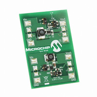
BOARD EVAL FOR MCP1640
Manufacturer
Microchip Technology
Type
DC/DC Switching Converters, Regulators & Controllersr
Datasheets
1.MCP1640CT-ICHY.pdf
(32 pages)
2.MCP1640CT-ICHY.pdf
(26 pages)
3.MCP1640EV-SBC.pdf
(22 pages)
Specifications of MCP1640EV-SBC
Main Purpose
DC/DC, Step Up
Outputs And Type
1, Non-Isolated
Voltage - Output
2V, 3.3V or 5V
Current - Output
100mA, 350mA
Voltage - Input
0.35 ~ 5.5V
Regulator Topology
Boost
Frequency - Switching
500kHz
Board Type
Fully Populated
Utilized Ic / Part
MCP1640
Input Voltage
0.35 V to 5.5 V
Output Voltage
3.3 V to 5 V
Operating Supply Voltage
0.35 V to 5.5 V
Product
Power Management Modules
Supply Current
300 mA
Kit Contents
Board
Features
Automatic PFM/PWM Operation, Enable State Selectable Using Mini-Dip Switch On Board
Svhc
No SVHC (15-Dec-2010)
Core Architecture
Power Management - Voltage Regulator
Rohs Compliant
Yes
For Use With/related Products
MCP1640
Lead Free Status / RoHS Status
Contains lead / RoHS non-compliant
Power - Output
-
Lead Free Status / Rohs Status
Lead free / RoHS Compliant
Available stocks
Company
Part Number
Manufacturer
Quantity
Price
Company:

Part Number:
MCP1640EV-SBC
Manufacturer:
Microchip Technology
Quantity:
135
Company:
Part Number:
MCP1640EV-SBC
Manufacturer:
MICROCHIP
Quantity:
12 000


4.2.2
In normal PWM operation, the MCP1640/B/C/D
operates as a fixed frequency, synchronous boost
converter. The switching frequency is internally
maintained with a precision oscillator typically set to
500 kHz. The MCP1640B/D devices will operate in
PWM only mode even during periods of light load
operation. By operating in PWM only mode, the output
ripple remains low and the frequency is constant.
Operating in fixed PWM mode results in lower
efficiency during light load operation (when compared
to PFM mode (MCP1640/C)).
Lossless current sensing converts the peak current sig-
nal to a voltage to sum with the internal slope compen-
sation. This summed signal is compared to the voltage
error amplifier output to provide a peak current control
command
compensation is adaptive to the input and output
voltage. Therefore, the converter provides the proper
amount of slope compensation to ensure stability, but is
not excessive, which causes a loss of phase margin.
The peak current limit is set to 800 mA typical.
4.2.3
The MCP1640/C devices are capable of operating in
normal PWM mode and PFM mode to maintain high
efficiency at all loads. In PFM mode, the output ripple
has a variable frequency component that changes with
the input voltage and output current. With no load, the
quiescent current draw from the output is typically
19 µA. The PFM mode can be disabled in selected
device options.
PFM operation is initiated if the output load current falls
below an internally programmed threshold. The output
voltage is continuously monitored. When the output
voltage drops below its nominal value, PFM operation
pulses one or several times to bring the output back
into regulation. If the output load current rises above
the upper threshold, the MCP1640/C transitions
smoothly into PWM mode.
4.2.4
The MCP1640/B/C/D output voltage is adjustable with
a resistor divider over a 2.0V minimum to 5.5V
maximum
recommended to minimize quiescent current to keep
efficiency high at light loads.
4.2.5
The enable pin is used to turn the boost converter on
and off. The enable threshold voltage varies with input
voltage. To enable the boost converter, the EN voltage
level must be greater than 90% of the V
disable the boost converter, the EN voltage must be
less than 20% of the V
2010 Microchip Technology Inc.
PWM MODE OPERATION
PFM MODE OPERATION
ADJUSTABLE OUTPUT VOLTAGE
ENABLE
for
range.
the
High
IN
PWM
voltage.
value
signal.
resistors
IN
The
voltage. To
slope
are
4.2.6
The MCP1640/B/C/D gets its start-up bias from V
Once the output exceeds the input, bias comes from
the output. Therefore, once started, operation is
completely independent of V
limited by the output power level and the input source
series resistance. Once started, the output will remain
in regulation down to 0.35V typical with 1 mA output
current for low source impedance inputs.
4.2.7
The error amplifier, with its associated compensation
network, completes the closed loop system by
comparing the output voltage to a reference at the
input of the error amplifier, and feeding the amplified
and inverted signal to the control input of the inner
current loop. The compensation network provides
phase leads and lags at appropriate frequencies to
cancel excessive phase lags and leads of the power
circuit. All necessary compensation components and
slope compensation are integrated.
4.2.8
Unlike most boost converters, the MCP1640/B/C/D
allows its output to be shorted during normal operation.
The internal current limit and overtemperature
protection limit excessive stress and protect the device
during periods of short circuit, overcurrent and over-
temperature. While operating in Bypass mode, the
P-Channel current limit is inhibited to minimize
quiescent current.
4.2.9
The MCP1640/B/C/D integrates a low noise anti-ring
switch that damps the oscillations typically observed at
the switch node of a boost converter when operating in
the discontinuous inductor current mode. This removes
the high frequency radiated noise.
4.2.10
Overtemperature protection circuitry is integrated in the
MCP1640/B/C/D. This circuitry monitors the device
junction temperature and shuts the device off if the
junction temperature exceeds the typical +150
threshold. If this threshold is exceeded, the device will
automatically restart once the junction temperature
drops by 10
overtemperature condition.
INTERNAL BIAS
INTERNAL COMPENSATION
SHORT CIRCUIT PROTECTION
LOW NOISE OPERATION
OVERTEMPERATURE
PROTECTION
MCP1640/B/C/D
o
C. The soft start is reset during an
IN
. Operation is only
DS22234A-page 13
o
IN
C
.
Related parts for MCP1640EV-SBC
Image
Part Number
Description
Manufacturer
Datasheet
Request
R

Part Number:
Description:
0.65V Start-up Synchronous Boost Regulator with True Output Disconnect or Input/Output Bypass Option
Manufacturer:
MICROCHIP [Microchip Technology]
Datasheet:

Part Number:
Description:
IC CONV DC-DC STEPUP SYNC 8DFN
Manufacturer:
Microchip Technology
Datasheet:

Part Number:
Description:
0.65v Start-up Synchronous Boost Regulator With True Output Disconnect Or Input/output Bypass Option
Manufacturer:
Microchip Technology Inc.
Datasheet:
Part Number:
Description:
Manufacturer:
Microchip Technology Inc.
Datasheet:
Part Number:
Description:
Manufacturer:
Microchip Technology Inc.
Datasheet:
Part Number:
Description:
Manufacturer:
Microchip Technology Inc.
Datasheet:
Part Number:
Description:
Manufacturer:
Microchip Technology Inc.
Datasheet:
Part Number:
Description:
Manufacturer:
Microchip Technology Inc.
Datasheet:
Part Number:
Description:
Manufacturer:
Microchip Technology Inc.
Datasheet:
Part Number:
Description:
Manufacturer:
Microchip Technology Inc.
Datasheet: