EVL6566A-75WADP STMicroelectronics, EVL6566A-75WADP Datasheet - Page 22
EVL6566A-75WADP
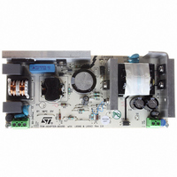
Manufacturer Part Number
EVL6566A-75WADP
Description
BOARD EVAL FOR L6566A
Manufacturer
STMicroelectronics
Type
Power Factor Correctionr
Datasheets
1.L6566ATR.pdf
(51 pages)
2.TSM1014IDT.pdf
(10 pages)
3.L6563ATR.pdf
(39 pages)
4.EVL6566A-75WADP.pdf
(8 pages)
Specifications of EVL6566A-75WADP
Main Purpose
AC/DC, Primary and Secondary Side with PFC
Outputs And Type
1, Isolated
Power - Output
75W
Voltage - Output
19V
Current - Output
4A
Voltage - Input
90 ~ 264VAC
Frequency - Switching
65kHz
Board Type
Fully Populated
Utilized Ic / Part
L6563, L6566A, TSM1014
Input Voltage
90 V to 264 V
Output Voltage
19 V
Dimensions
78 mm x 174 mm
Product
Power Management Modules
Lead Free Status / RoHS Status
Lead free / RoHS Compliant
Regulator Topology
-
Lead Free Status / Rohs Status
Lead free / RoHS Compliant
For Use With/related Products
L6563, L6566A
Other names
497-6449
Available stocks
Company
Part Number
Manufacturer
Quantity
Price


Application information
22/39
Figure 38. THD optimization: standard TM PFC controller (left side) and L6563/A
Essentially, the circuit artificially increases the ON-time of the power switch with a positive
offset added to the output of the multiplier in the proximity of the line voltage zero-crossings.
This offset is reduced as the instantaneous line voltage increases, so that it becomes
negligible as the line voltage moves toward the top of the sinusoid. Furthermore the offset is
modulated by the voltage on the V
little offset at low line, where energy transfer at zero crossings is typically quite good, and a
larger offset at high line where the energy transfer gets worse.
The effect of the circuit is shown in
PFC controller are compared to those of this chip.
To take maximum benefit from the THD optimizer circuit, the high-frequency filter capacitor
after the bridge rectifier should be minimized, compatibly with EMI filtering needs. A large
capacitance, in fact, introduces a conduction dead-angle of the AC input current in itself -
even with an ideal energy transfer by the PFC pre-regulator - thus reducing the effectiveness
of the optimizer circuit.
Imains
Input current
(right side)
Rectified mains voltage
MOSFET's drain voltage
Input current
FF
Vdrain
Figure
pin (see
38, where the key waveforms of a standard TM
Section 6.3 on page 18
Imains
Input current
Rectified mains voltage
section) so as to have
MOSFET's drain voltage
Input current
L6563 - L6563A
Vdrain
Related parts for EVL6566A-75WADP
Image
Part Number
Description
Manufacturer
Datasheet
Request
R

Part Number:
Description:
BOARD DEMO FOR L6563/LL6566A
Manufacturer:
STMicroelectronics
Datasheet:

Part Number:
Description:
STMicroelectronics [RIPPLE-CARRY BINARY COUNTER/DIVIDERS]
Manufacturer:
STMicroelectronics
Datasheet:
Part Number:
Description:
STMicroelectronics [LIQUID-CRYSTAL DISPLAY DRIVERS]
Manufacturer:
STMicroelectronics
Datasheet:

Part Number:
Description:
BOARD EVAL FOR MEMS SENSORS
Manufacturer:
STMicroelectronics
Datasheet:
Part Number:
Description:
NPN TRANSISTOR POWER MODULE
Manufacturer:
STMicroelectronics
Datasheet:
Part Number:
Description:
TURBOSWITCH ULTRA-FAST HIGH VOLTAGE DIODE
Manufacturer:
STMicroelectronics
Datasheet:
Part Number:
Description:
Manufacturer:
STMicroelectronics
Datasheet:
Part Number:
Description:
DIODE / SCR MODULE
Manufacturer:
STMicroelectronics
Datasheet:
Part Number:
Description:
DIODE / SCR MODULE
Manufacturer:
STMicroelectronics
Datasheet:
Part Number:
Description:
Search -----> STE16N100
Manufacturer:
STMicroelectronics
Datasheet:
Part Number:
Description:
Search ---> STE53NA50
Manufacturer:
STMicroelectronics
Datasheet:
Part Number:
Description:
NPN Transistor Power Module
Manufacturer:
STMicroelectronics
Datasheet: