EVL6566A-75WADP STMicroelectronics, EVL6566A-75WADP Datasheet - Page 23
EVL6566A-75WADP
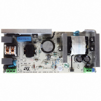
Manufacturer Part Number
EVL6566A-75WADP
Description
BOARD EVAL FOR L6566A
Manufacturer
STMicroelectronics
Type
Power Factor Correctionr
Datasheets
1.L6566ATR.pdf
(51 pages)
2.TSM1014IDT.pdf
(10 pages)
3.L6563ATR.pdf
(39 pages)
4.EVL6566A-75WADP.pdf
(8 pages)
Specifications of EVL6566A-75WADP
Main Purpose
AC/DC, Primary and Secondary Side with PFC
Outputs And Type
1, Isolated
Power - Output
75W
Voltage - Output
19V
Current - Output
4A
Voltage - Input
90 ~ 264VAC
Frequency - Switching
65kHz
Board Type
Fully Populated
Utilized Ic / Part
L6563, L6566A, TSM1014
Input Voltage
90 V to 264 V
Output Voltage
19 V
Dimensions
78 mm x 174 mm
Product
Power Management Modules
Lead Free Status / RoHS Status
Lead free / RoHS Compliant
Regulator Topology
-
Lead Free Status / Rohs Status
Lead free / RoHS Compliant
For Use With/related Products
L6563, L6566A
Other names
497-6449
Available stocks
Company
Part Number
Manufacturer
Quantity
Price


L6563 - L6563A
6.5
Tracking Boost function
In some applications it may be advantageous to regulate the output voltage of the PFC pre-
regulator so that it tracks the RMS input voltage rather than at a fixed value like in
conventional boost pre-regulators. This is commonly referred to as "tracking boost" or
"follower boost" approach.
With this IC the function can be realized by connecting a resistor (R
and ground. The TBO pin presents a DC level equal to the peak of the MULT pin voltage and
is then representative of the mains RMS voltage. The resistor defines a current, equal to
V(TBO)/R
amplifier. In this way, when the mains voltage increases the voltage at TBO pin will increase
as well and so will do the current flowing through the resistor connected between TBO and
GND. Then a larger current will be sunk by INV pin and the output voltage of the PFC pre-
regulator will be forced to get higher. Obviously, the output voltage will move in the opposite
direction if the input voltage decreases.
To avoid undesired output voltage rise should the mains voltage exceed the maximum
specified value, the voltage at the TBO pin is clamped at 3V. By properly selecting the
multiplier bias it is possible to set the maximum input voltage above which input-to-output
tracking ends and the output voltage becomes constant. If this function is not used, leave
the pin open: the device will regulate a fixed output voltage.
Starting from the following data:
●
●
●
●
●
●
Vin
Vin
Vo
Vo
Vox = absolute maximum limit for the regulated output voltage;
∆Vo = OVP threshold,
1
2
1
2
= regulated output voltage @ Vin = Vin
= regulated output voltage @ Vin = Vin
= minimum specified input RMS voltage;
= maximum specified input RMS voltage;
T
, that is internally 1:1 mirrored and sunk from pin INV (pin 1) input of the error
1
2
;
;
Application information
T
) between the TBO pin
23/39
Related parts for EVL6566A-75WADP
Image
Part Number
Description
Manufacturer
Datasheet
Request
R

Part Number:
Description:
BOARD DEMO FOR L6563/LL6566A
Manufacturer:
STMicroelectronics
Datasheet:

Part Number:
Description:
STMicroelectronics [RIPPLE-CARRY BINARY COUNTER/DIVIDERS]
Manufacturer:
STMicroelectronics
Datasheet:
Part Number:
Description:
STMicroelectronics [LIQUID-CRYSTAL DISPLAY DRIVERS]
Manufacturer:
STMicroelectronics
Datasheet:

Part Number:
Description:
BOARD EVAL FOR MEMS SENSORS
Manufacturer:
STMicroelectronics
Datasheet:
Part Number:
Description:
NPN TRANSISTOR POWER MODULE
Manufacturer:
STMicroelectronics
Datasheet:
Part Number:
Description:
TURBOSWITCH ULTRA-FAST HIGH VOLTAGE DIODE
Manufacturer:
STMicroelectronics
Datasheet:
Part Number:
Description:
Manufacturer:
STMicroelectronics
Datasheet:
Part Number:
Description:
DIODE / SCR MODULE
Manufacturer:
STMicroelectronics
Datasheet:
Part Number:
Description:
DIODE / SCR MODULE
Manufacturer:
STMicroelectronics
Datasheet:
Part Number:
Description:
Search -----> STE16N100
Manufacturer:
STMicroelectronics
Datasheet:
Part Number:
Description:
Search ---> STE53NA50
Manufacturer:
STMicroelectronics
Datasheet:
Part Number:
Description:
NPN Transistor Power Module
Manufacturer:
STMicroelectronics
Datasheet: