AG920-07E NVE, AG920-07E Datasheet - Page 81
AG920-07E
Manufacturer Part Number
AG920-07E
Description
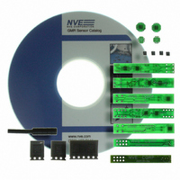
KIT EVALUATION GT SENSOR
Manufacturer
NVE
Specifications of AG920-07E
Sensor Type
Magnetic. GMR (Giant Magnetoresistive)
Interface
Analog
Embedded
No
Utilized Ic / Part
ABL & AKL Series GT Sensors
Lead Free Status / RoHS Status
Lead free / RoHS Compliant
Voltage - Supply
-
Sensitivity
-
Sensing Range
-
Other names
391-1063


Application Notes
The figure below shows a simplified structure of a typical GMR sensor film, as manufactured by NVE:
Cross Sectional Structure of Basic GMR Material
Top Film (Magnetic Material, 20-50 Angstroms Thick)
Conductive Interlayer (Non-Magnetic Material, 15-40 Angstroms Thick)
Bottom Film (Magnetic Material, 20-50 Angstroms Thick)
The diagram shows two magnetic material layers, sandwiching a non-magnetic interlayer. The
magnetic layers are designed to have anti-ferromagnetic coupling. This means that the magnetization
of these layers is opposite to each other when there is no external magnetic field applied to the
material. Antiferromagnetic coupling can be visualized by imagining two bar magnets on either side of
a thin sheet of plastic. The magnets couple head to tail (north pole to south pole) across the boundary
formed by the plastic. In a similar fashion, the magnetization direction of the magnetic layers in the
GMR film couple head to tail across the non-magnetic interlayer of the film.
The conduction electrons in magnetic materials have a spin characteristic. The electrons are normally
referred to as spin up electrons when the material is magnetized in one direction, and spin down
electrons when the material is magnetized in the opposite direction.
The diagram below shows some electron paths inside the GMR material structure. The two arrows
indicate the antiferromagnetic coupling. Notice that the electrons tend to scatter off the two GMR
material interfaces. This is because the electrons from the spin up layer are trying to enter the spin
down layer, and vice versa. Because of the differences in the electron spins, it is more likely that the
electrons will scatter at these interfaces:
Spin UP Electrons Scatter at Interface with Spin DOWN Layer;
Spin DOWN Electrons Scatter at Interface with Spin UP Layer
Average Mean Free Path of the Electrons is Short
Magnetization Direction of Top Film
Top Film
(Primarily Spin UP Electrons,
Due to Magnetization Direction)
Conductive Interlayer
Bottom Film
(Primarily Spin DOWN Electrons,
Due to Magnetization Direction)
Magnetization Direction of Bottom Film
- 81 -
www.nve.com
phone: 952-829-9217 fax: 952-829-9189
Related parts for AG920-07E
Image
Part Number
Description
Manufacturer
Datasheet
Request
R

Part Number:
Description:
KIT EVALUATION GT SENSOR
Manufacturer:
NVE
Datasheet:

Part Number:
Description:
ISOLATOR HS MAG DIGITAL 8SOIC
Manufacturer:
NVE
Datasheet:
Part Number:
Description:
ISOLATOR HS DIGITAL 125C 8SOIC
Manufacturer:
NVE
Datasheet:

Part Number:
Description:
HI-SPD 4CHANN COUPLER 16-SOIC LF
Manufacturer:
NVE
Datasheet:
Part Number:
Description:
ISOLATOR HS MAG DIGITAL 16SOIC
Manufacturer:
NVE
Datasheet:
Part Number:
Description:
ISOLATOR HS MAG DIGITAL 8SOIC
Manufacturer:
NVE
Datasheet:
Part Number:
Description:
IC DIFFER BUS TRANSC 16 SOIC
Manufacturer:
NVE
Datasheet:
Part Number:
Description:
ISOLATOR HS MAG DIGITAL 16SOICW
Manufacturer:
NVE
Datasheet:

Part Number:
Description:
ISOLATOR RS422/485 INTFC 16SOICW
Manufacturer:
NVE
Datasheet:
Part Number:
Description:
ISOLATOR HS MAG DIGITAL 16SOICW
Manufacturer:
NVE
Datasheet:

Part Number:
Description:
IC, DIGITAL ISOLATOR, 12NS, NSOIC-8
Manufacturer:
NVE
Datasheet:

Part Number:
Description:
IC, DIGITAL ISOLATOR, 12NS, DIP-8
Manufacturer:
NVE
Datasheet:
Part Number:
Description:
IC TXRX ISOLATED CAN HS 16SOIC
Manufacturer:
NVE
Datasheet: