DV164136 Microchip Technology, DV164136 Datasheet - Page 140
DV164136
Manufacturer Part Number
DV164136
Description
DEVELOPMENT KIT FOR PIC18
Manufacturer
Microchip Technology
Series
PIC®r
Type
MCUr
Datasheets
1.DM183032.pdf
(38 pages)
2.DV164136.pdf
(448 pages)
3.DV164136.pdf
(6 pages)
4.DV164136.pdf
(446 pages)
5.DV164136.pdf
(4 pages)
6.DV164136.pdf
(18 pages)
Specifications of DV164136
Contents
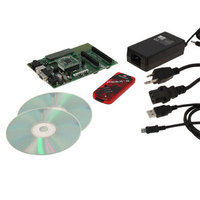
Board, Cables, CDs, PICkit™ 3 Programmer, Power Supply
Processor To Be Evaluated
PIC18F8722, PIC18F87J11
Interface Type
RS-232, USB
Operating Supply Voltage
3.3 V, 5 V
Silicon Manufacturer
Microchip
Core Architecture
PIC
Core Sub-architecture
PIC18
Silicon Core Number
PIC18F
Silicon Family Name
PIC18F8xxx
Kit Contents
PIC18 Exp Brd PICkit 3 Cable CD PSU
Lead Free Status / RoHS Status
Lead free / RoHS Compliant
For Use With/related Products
PIC18F8722, PIC18F87J11
Lead Free Status / Rohs Status
Lead free / RoHS Compliant
Available stocks
Company
Part Number
Manufacturer
Quantity
Price
Company:

Part Number:
DV164136
Manufacturer:
MICROCHIP
Quantity:
12 000


PIC18F87J11 FAMILY
TABLE 10-10: PORTD FUNCTIONS (CONTINUED)
TABLE 10-11: SUMMARY OF REGISTERS ASSOCIATED WITH PORTD
DS39778D-page 140
PORTD
LATD
TRISD
PORTG
Legend: Shaded cells are not used by PORTD.
Note 1:
RD6/AD6/
PMD6/SCK2/
SCL2
RD7/AD7/
PMD7/SS2
Legend:
Note 1:
Pin Name
Name
2:
3:
Unimplemented on 64-pin devices, read as ‘0’.
O = Output, I = Input, DIG = Digital Output, ST = Schmitt Buffer Input, TTL = TTL Buffer Input,
x = Don’t care (TRIS bit does not affect port direction or is overridden for this option).
External memory interface I/O takes priority over all other digital and PMP I/O.
Available on 80-pin devices only.
Default configuration for PMP (PMPMX Configuration bit = 1).
TRISD7
LATD7
RDPU
Bit 7
RD7
Function
PMD6
PMD7
AD6
AD7
SCK2
SCL2
RD6
RD7
SS2
(2)
(2)
(3)
(3)
TRISD6
LATD6
REPU
Bit 6
RD6
Setting
TRIS
0
1
x
x
x
x
0
1
0
1
0
1
x
x
x
x
x
RJPU
TRISD5
LATD5
Bit 5
I/O
RD5
O
O
O
O
O
O
O
O
I
I
I
I
I
I
I
I
I
(1)
DIG-3
Type
DIG
TTL
DIG
TTL
DIG
DIG
DIG
DIG
TTL
DIG
TTL
TTL
I/O
ST
ST
ST
ST
TRISD4
LATD4
Bit 4
RD4
RG4
LATD<6> data output.
PORTD<6> data input.
External memory interface, address/data bit 6 output.
External memory interface, data bit 6 input.
Parallel Master Port data out.
Parallel Master Port data input.
SPI clock output (MSSP2 module); takes priority over port data.
SPI clock input (MSSP2 module).
I
I
setting.
LATD<7> data output.
PORTD<7> data input.
External memory interface, address/data bit 7 output.
External memory interface, data bit 7 input.
Parallel Master Port data out.
Parallel Master Port data input.
Slave select input for MSSP2 module.
2
2
C™ clock output (MSSP2 module); takes priority over port data.
C clock input (MSSP2 module); input type depends on module
TRISD3
LATD3
Bit 3
RD3
RG3
TRISD2
LATD2
Bit 2
RD2
RG2
Description
TRISD1
LATD1
Bit 1
RD1
RG1
© 2009 Microchip Technology Inc.
(1)
(1)
TRISD0
LATD0
Bit 0
RD0
RG0
(1)
(1)
on Page:
Values
Reset
61
60
60
61
Related parts for DV164136
Image
Part Number
Description
Manufacturer
Datasheet
Request
R

Part Number:
Description:
Manufacturer:
Microchip Technology Inc.
Datasheet:
Part Number:
Description:
Manufacturer:
Microchip Technology Inc.
Datasheet:
Part Number:
Description:
Manufacturer:
Microchip Technology Inc.
Datasheet:
Part Number:
Description:
Manufacturer:
Microchip Technology Inc.
Datasheet:
Part Number:
Description:
Manufacturer:
Microchip Technology Inc.
Datasheet:
Part Number:
Description:
Manufacturer:
Microchip Technology Inc.
Datasheet:
Part Number:
Description:
Manufacturer:
Microchip Technology Inc.
Datasheet:
Part Number:
Description:
Manufacturer:
Microchip Technology Inc.
Datasheet: