DV164136 Microchip Technology, DV164136 Datasheet - Page 293
DV164136
Manufacturer Part Number
DV164136
Description
DEVELOPMENT KIT FOR PIC18
Manufacturer
Microchip Technology
Series
PIC®r
Type
MCUr
Datasheets
1.DM183032.pdf
(38 pages)
2.DV164136.pdf
(448 pages)
3.DV164136.pdf
(6 pages)
4.DV164136.pdf
(446 pages)
5.DV164136.pdf
(4 pages)
6.DV164136.pdf
(18 pages)
Specifications of DV164136
Contents
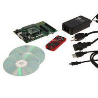
Board, Cables, CDs, PICkit™ 3 Programmer, Power Supply
Processor To Be Evaluated
PIC18F8722, PIC18F87J11
Interface Type
RS-232, USB
Operating Supply Voltage
3.3 V, 5 V
Silicon Manufacturer
Microchip
Core Architecture
PIC
Core Sub-architecture
PIC18
Silicon Core Number
PIC18F
Silicon Family Name
PIC18F8xxx
Kit Contents
PIC18 Exp Brd PICkit 3 Cable CD PSU
Lead Free Status / RoHS Status
Lead free / RoHS Compliant
For Use With/related Products
PIC18F8722, PIC18F87J11
Lead Free Status / Rohs Status
Lead free / RoHS Compliant
Available stocks
Company
Part Number
Manufacturer
Quantity
Price
Company:

Part Number:
DV164136
Manufacturer:
MICROCHIP
Quantity:
12 000


21.0
The Analog-to-Digital (A/D) Converter module has
11 inputs for the 64-pin devices and 15 for the 80-pin
devices. This module allows conversion of an analog
input signal to a corresponding 10-bit digital number.
The module has six registers:
• A/D Control Register 0 (ADCON0)
• A/D Control Register 1 (ADCON1)
REGISTER 21-1:
© 2009 Microchip Technology Inc.
bit 7
Legend:
R = Readable bit
-n = Value at POR
bit 7-6
bit
bit 5-2
bit 1
bit 0
Note 1:
VCFG1
R/W-0
2:
3:
10-BIT ANALOG-TO-DIGITAL
CONVERTER (A/D) MODULE
Default (legacy) SFR at this address, available when WDTCON<4> = 0.
These channels are not implemented on 64-pin devices.
Performing a conversion on unimplemented channels will return random values.
VCFG1: Voltage Reference Configuration bit (V
1 = V
0 = AV
VCFG0: Voltage Reference Configuration bit (V
1 = V
0 = AV
CHS3:CHS0: Analog Channel Select bits
0000 = Channel 00 (AN0)
0001 = Channel 01 (AN1)
0010 = Channel 02 (AN2)
0011 = Channel 03 (AN3)
0100 = Channel 04 (AN4)
0101 = Unused
0110 = Channel 06 (AN6)
0111 = Channel 07 (AN7)
1000 = Channel 08 (AN8)
1001 = Channel 09 (AN9)
1010 = Channel 10 (AN10)
1011 = Channel 11 (AN11)
1100 = Channel 12 (AN12)
1101 = Channel 13 (AN13)
1110 = Channel 14 (AN14)
1111 = Channel 15 (AN15)
GO/DONE: A/D Conversion Status bit
When ADON = 1:
1 = A/D conversion in progress
0 = A/D Idle
ADON: A/D On bit
1 = A/D Converter module is enabled
0 = A/D Converter module is disabled
VCFG0
R/W-0
REF
REF
SS
DD
ADCON0: A/D CONTROL REGISTER 0
- (AN2)
+ (AN3)
W = Writable bit
‘1’ = Bit is set
R/W-0
CHS3
(2,3)
(2,3)
(2,3)
(2,3)
R/W-0
CHS2
U = Unimplemented bit, read as ‘0’
‘0’ = Bit is cleared
PIC18F87J11 FAMILY
REF
REF
R/W-0
CHS1
• A/D Port Configuration Register 2 (ANCON0)
• A/D Port Configuration Register 1 (ANCON1)
• A/D Result Registers (ADRESH and ADRESL)
The ADCON0 register, shown in Register 21-1,
controls the operation of the A/D module. The
ADCON1 register, shown in Register 21-2, configures
the A/D clock source, programmed acquisition time and
justification.
- source)
+ source)
(1)
R/W-0
CHS0
x = Bit is unknown
GO/DONE
R/W-0
DS39778D-page 293
ADON
R/W-0
bit 0
Related parts for DV164136
Image
Part Number
Description
Manufacturer
Datasheet
Request
R

Part Number:
Description:
Manufacturer:
Microchip Technology Inc.
Datasheet:
Part Number:
Description:
Manufacturer:
Microchip Technology Inc.
Datasheet:
Part Number:
Description:
Manufacturer:
Microchip Technology Inc.
Datasheet:
Part Number:
Description:
Manufacturer:
Microchip Technology Inc.
Datasheet:
Part Number:
Description:
Manufacturer:
Microchip Technology Inc.
Datasheet:
Part Number:
Description:
Manufacturer:
Microchip Technology Inc.
Datasheet:
Part Number:
Description:
Manufacturer:
Microchip Technology Inc.
Datasheet:
Part Number:
Description:
Manufacturer:
Microchip Technology Inc.
Datasheet: