DV164136 Microchip Technology, DV164136 Datasheet - Page 22
DV164136
Manufacturer Part Number
DV164136
Description
DEVELOPMENT KIT FOR PIC18
Manufacturer
Microchip Technology
Series
PIC®r
Type
MCUr
Datasheets
1.DM183032.pdf
(38 pages)
2.DV164136.pdf
(448 pages)
3.DV164136.pdf
(6 pages)
4.DV164136.pdf
(446 pages)
5.DV164136.pdf
(4 pages)
6.DV164136.pdf
(18 pages)
Specifications of DV164136
Contents
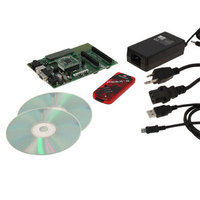
Board, Cables, CDs, PICkit™ 3 Programmer, Power Supply
Processor To Be Evaluated
PIC18F8722, PIC18F87J11
Interface Type
RS-232, USB
Operating Supply Voltage
3.3 V, 5 V
Silicon Manufacturer
Microchip
Core Architecture
PIC
Core Sub-architecture
PIC18
Silicon Core Number
PIC18F
Silicon Family Name
PIC18F8xxx
Kit Contents
PIC18 Exp Brd PICkit 3 Cable CD PSU
Lead Free Status / RoHS Status
Lead free / RoHS Compliant
For Use With/related Products
PIC18F8722, PIC18F87J11
Lead Free Status / Rohs Status
Lead free / RoHS Compliant
Available stocks
Company
Part Number
Manufacturer
Quantity
Price
Company:

Part Number:
DV164136
Manufacturer:
MICROCHIP
Quantity:
12 000


PIC18F87J11 FAMILY
TABLE 1-4:
DS39778D-page 22
MCLR
OSC1/CLKI/RA7
OSC2/CLKO/RA6
Legend: TTL = TTL compatible input
Note 1: Alternate assignment for ECCP2/P2A when Configuration bit, CCP2MX, is cleared (Extended Microcontroller mode).
OSC1
CLKI
RA7
OSC2
CLKO
RA6
2: Default assignment for ECCP2/P2A for all devices in all operating modes (CCP2MX is set).
3: Default assignments for P1B/P1C/P3B/P3C (ECCPMX Configuration bit is set).
4: Alternate assignment for ECCP2/P2A when CCP2MX is cleared (Microcontroller mode).
5: Alternate assignments for P1B/P1C/P3B/P3C (ECCPMX Configuration bit is cleared).
6: Default assignment for PMP data and control pins when PMPMX Configuration bit is set.
7: Alternate assignment for PMP data and control pins when PMPMX Configuration bit is cleared (programmed).
Pin Name
ST = Schmitt Trigger input with CMOS levels
I
P
= Input
= Power
PIC18F8XJ1X PINOUT I/O DESCRIPTIONS
Pin Number
80-TQFP
49
50
9
Type
Pin
I/O
I/O
O
O
I
I
I
Buffer
CMOS
Type
TTL
TTL
ST
ST
—
—
Master Clear (Reset) input. This pin is an active-low Reset to
the device.
Oscillator crystal or external clock input. Available only in
external oscillator modes (EC/ECPLL and HS/HSPLL).
Main oscillator input connection.
Main clock input connection.
General purpose I/O pin. Available only in INTIO2 and
INTPLL2 Oscillator modes.
Oscillator crystal or clock output. Available only in external
oscillator modes (EC/ECPLL and HS/HSPLL).
Main oscillator feedback output connection.
System cycle clock output (F
General purpose I/O pin. Available only in INTIO and INTPLL
Oscillator modes.
Oscillator crystal input or external clock source input.
ST buffer when configured in RC mode; CMOS
otherwise.
External clock source input. Always associated
with pin function OSC1. (See related OSC1/CLKI,
OSC2/CLKO pins.)
Oscillator crystal output. Connects to crystal or
resonator in Crystal Oscillator mode.
In EC, ECPLL, INTIO1 and INTPLL1 Oscillator modes,
OSC2 pin outputs CLKO which has 1/4 the frequency
of OSC1 and denotes the instruction cycle rate.
CMOS = CMOS compatible input or output
Analog = Analog input
O
OD
= Output
= Open-Drain (no P diode to V
Description
OSC
© 2009 Microchip Technology Inc.
/4).
DD
)
Related parts for DV164136
Image
Part Number
Description
Manufacturer
Datasheet
Request
R

Part Number:
Description:
Manufacturer:
Microchip Technology Inc.
Datasheet:
Part Number:
Description:
Manufacturer:
Microchip Technology Inc.
Datasheet:
Part Number:
Description:
Manufacturer:
Microchip Technology Inc.
Datasheet:
Part Number:
Description:
Manufacturer:
Microchip Technology Inc.
Datasheet:
Part Number:
Description:
Manufacturer:
Microchip Technology Inc.
Datasheet:
Part Number:
Description:
Manufacturer:
Microchip Technology Inc.
Datasheet:
Part Number:
Description:
Manufacturer:
Microchip Technology Inc.
Datasheet:
Part Number:
Description:
Manufacturer:
Microchip Technology Inc.
Datasheet: