DV164136 Microchip Technology, DV164136 Datasheet - Page 197
DV164136
Manufacturer Part Number
DV164136
Description
DEVELOPMENT KIT FOR PIC18
Manufacturer
Microchip Technology
Series
PIC®r
Type
MCUr
Datasheets
1.DM183032.pdf
(38 pages)
2.DV164136.pdf
(448 pages)
3.DV164136.pdf
(6 pages)
4.DV164136.pdf
(446 pages)
5.DV164136.pdf
(4 pages)
6.DV164136.pdf
(18 pages)
Specifications of DV164136
Contents
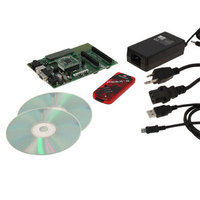
Board, Cables, CDs, PICkit™ 3 Programmer, Power Supply
Processor To Be Evaluated
PIC18F8722, PIC18F87J11
Interface Type
RS-232, USB
Operating Supply Voltage
3.3 V, 5 V
Silicon Manufacturer
Microchip
Core Architecture
PIC
Core Sub-architecture
PIC18
Silicon Core Number
PIC18F
Silicon Family Name
PIC18F8xxx
Kit Contents
PIC18 Exp Brd PICkit 3 Cable CD PSU
Lead Free Status / RoHS Status
Lead free / RoHS Compliant
For Use With/related Products
PIC18F8722, PIC18F87J11
Lead Free Status / Rohs Status
Lead free / RoHS Compliant
Available stocks
Company
Part Number
Manufacturer
Quantity
Price
Company:

Part Number:
DV164136
Manufacturer:
MICROCHIP
Quantity:
12 000


17.0
Members of the PIC18F87J11 family of devices all have
a total of five CCP (Capture/Compare/PWM) modules.
Two of these (CCP4 and CCP5) implement standard
Capture, Compare and Pulse-Width Modulation (PWM)
modes and are discussed in this section. The other three
modules
standard Capture and Compare modes, as well as
Enhanced PWM modes. These are discussed in
Section 18.0
(ECCP) Module”.
Each CCP/ECCP module contains a 16-bit register
which can operate as a 16-bit Capture register, a 16-bit
Compare register or a PWM Master/Slave Duty Cycle
register. For the sake of clarity, all CCP module opera-
tion in the following sections is described with respect
to CCP4, but is equally applicable to CCP5.
REGISTER 17-1:
© 2009 Microchip Technology Inc.
bit 7
Legend:
R = Readable bit
-n = Value at POR
bit 7-6
bit 5-4
bit 3-0
U-0
—
CAPTURE/COMPARE/PWM
(CCP) MODULES
(ECCP1,
Unimplemented: Read as ‘0’
CCPx<X:Y>: PWM Duty Cycle bit 1 and bit 0 for CCPx Module
Capture mode:
Unused.
Compare mode:
Unused.
PWM mode:
These bits are the two Least Significant bits (bit 1 and bit 0) of the 10-bit PWM duty cycle. The eight Most
Significant bits (DCx9:DCx2) of the duty cycle are found in CCPRxL.
CCPxM3:CCPxM0: CCPx Module Mode Select bits
0000 = Capture/Compare/PWM disabled (resets CCPx module)
0001 = Reserved
0010 = Compare mode, toggle output on match (CCPxIF bit is set)
0011 = Reserved
0100 = Capture mode: every falling edge
0101 = Capture mode: every rising edge
0110 = Capture mode: every 4th rising edge
0111 = Capture mode: every 16th rising edge
1000 = Compare mode: initialize CCPx pin low; on compare match, force CCPx pin high (CCPxIF bit is set)
1001 = Compare mode: initialize CCPx pin high; on compare match, force CCPx pin low (CCPxIF bit is set)
1010 = Compare mode: generate software interrupt on compare match (CCPxIF bit is set,
1011 = Compare mode: trigger special event, reset timer, start A/D conversion on CCPx match
11xx = PWM mode
“Enhanced
U-0
—
ECCP2,
CCPx pin reflects I/O state)
(CCPxIF bit is set)
CCPxCON: CCPx CONTROL REGISTER (CCP4 MODULE, CCP5 MODULE)
W = Writable bit
‘1’ = Bit is set
Capture/Compare/PWM
CCPxX
R/W-0
ECCP3)
(1)
implement
CCPxY
R/W-0
U = Unimplemented bit, read as ‘0’
‘0’ = Bit is cleared
CCPxM3
PIC18F87J11 FAMILY
R/W-0
Capture and Compare operations described in this
chapter apply to all standard and Enhanced CCP
modules. The operations of PWM mode, described in
Section 17.4 “PWM Mode”, apply to CCP4 and CCP5
only.
Note: Throughout this section and Section 18.0
“Enhanced Capture/Compare/PWM (ECCP)
Module”, references to register and bit names
that may be associated with a specific CCP
module are referred to generically by the use of
‘x’ or ‘y’ in place of the specific module number.
Thus, “CCPxCON” might refer to the control
register for ECCP1, ECCP2, ECCP3, CCP4 or
CCP5.
CCPxM2
R/W-0
x = Bit is unknown
CCPxM1
R/W-0
DS39778D-page 197
CCPxM0
R/W-0
bit 0
Related parts for DV164136
Image
Part Number
Description
Manufacturer
Datasheet
Request
R

Part Number:
Description:
Manufacturer:
Microchip Technology Inc.
Datasheet:
Part Number:
Description:
Manufacturer:
Microchip Technology Inc.
Datasheet:
Part Number:
Description:
Manufacturer:
Microchip Technology Inc.
Datasheet:
Part Number:
Description:
Manufacturer:
Microchip Technology Inc.
Datasheet:
Part Number:
Description:
Manufacturer:
Microchip Technology Inc.
Datasheet:
Part Number:
Description:
Manufacturer:
Microchip Technology Inc.
Datasheet:
Part Number:
Description:
Manufacturer:
Microchip Technology Inc.
Datasheet:
Part Number:
Description:
Manufacturer:
Microchip Technology Inc.
Datasheet: