DV164136 Microchip Technology, DV164136 Datasheet - Page 210
DV164136
Manufacturer Part Number
DV164136
Description
DEVELOPMENT KIT FOR PIC18
Manufacturer
Microchip Technology
Series
PIC®r
Type
MCUr
Datasheets
1.DM183032.pdf
(38 pages)
2.DV164136.pdf
(448 pages)
3.DV164136.pdf
(6 pages)
4.DV164136.pdf
(446 pages)
5.DV164136.pdf
(4 pages)
6.DV164136.pdf
(18 pages)
Specifications of DV164136
Contents
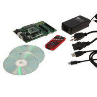
Board, Cables, CDs, PICkit™ 3 Programmer, Power Supply
Processor To Be Evaluated
PIC18F8722, PIC18F87J11
Interface Type
RS-232, USB
Operating Supply Voltage
3.3 V, 5 V
Silicon Manufacturer
Microchip
Core Architecture
PIC
Core Sub-architecture
PIC18
Silicon Core Number
PIC18F
Silicon Family Name
PIC18F8xxx
Kit Contents
PIC18 Exp Brd PICkit 3 Cable CD PSU
Lead Free Status / RoHS Status
Lead free / RoHS Compliant
For Use With/related Products
PIC18F8722, PIC18F87J11
Lead Free Status / Rohs Status
Lead free / RoHS Compliant
Available stocks
Company
Part Number
Manufacturer
Quantity
Price
Company:

Part Number:
DV164136
Manufacturer:
MICROCHIP
Quantity:
12 000


PIC18F87J11 FAMILY
18.4
The Enhanced PWM mode provides additional PWM
output options for a broader range of control applica-
tions. The module is a backward compatible version of
the standard CCP module and offers up to four outputs,
designated PxA through PxD. Users are also able to
select the polarity of the signal (either active-high or
active-low). The module’s output mode and polarity
are configured by setting the PxM1:PxM0 and
CCPxM3:CCPxM0 bits of the CCPxCON register
(CCPxCON<7:6> and CCPxCON<3:0>, respectively).
For the sake of clarity, Enhanced PWM mode operation
is described generically throughout this section with
respect to the ECCP1 and TMR2 modules. Control reg-
ister names are presented in terms of ECCP1. All three
Enhanced modules, as well as the two timer resources,
can be used interchangeably and function identically.
TMR2 or TMR4 can be selected for PWM operation by
selecting the proper bits in T3CON.
Figure 18-1 shows a simplified block diagram of PWM
operation. All control registers are double-buffered and
are loaded at the beginning of a new PWM cycle (the
period boundary when Timer2 resets) in order to
prevent glitches on any of the outputs. The exception is
the ECCPx PWM Delay register, ECCPxDEL, which is
loaded at either the duty cycle boundary or the bound-
ary period (whichever comes first). Because of the
buffering, the module waits until the assigned timer
resets instead of starting immediately. This means that
FIGURE 18-1:
DS39778D-page 210
Note: The 8-bit TMR2 register is concatenated with the 2-bit internal Q clock, or 2 bits of the prescaler, to create the 10-bit time base.
Enhanced PWM Mode
CCPR1H (Slave)
Duty Cycle Registers
Comparator
CCPR1L
TMR2
PR2
Comparator
SIMPLIFIED BLOCK DIAGRAM OF THE ENHANCED PWM MODULE
(Note 1)
Clear Timer,
set ECCP1 pin and
latch D.C.
CCP1CON<5:4>
R
S
P1M1<1:0>
Q
ECCP1DEL
Controller
ECCP1/P1A
Output
Enhanced PWM waveforms do not exactly match the
standard PWM waveforms, but are instead offset by
one full instruction cycle (4 T
As before, the user must manually configure the
appropriate TRIS bits for output.
18.4.1
The PWM period is specified by writing to the PR2
register. The PWM period can be calculated using the
equation:
EQUATION 18-1:
PWM frequency is defined as 1/[PWM period]. When
TMR2 is equal to PR2, the following three events occur
on the next increment cycle:
• TMR2 is cleared
• The ECCP1 pin is set (if PWM duty cycle = 0%,
• The PWM duty cycle is copied from CCPR1L into
2
the ECCP1 pin will not be set)
CCPR1H
Note:
P1B
P1C
P1D
PWM Period = [(PR2) + 1] • 4 • T
CCP1M<3:0>
4
PWM PERIOD
The Timer2 postscaler (see Section 14.0
“Timer2 Module”) is not used in the
determination of the PWM frequency. The
postscaler could be used to have a servo
update rate at a different frequency than
the PWM output.
TRISx<x>
TRISx<x>
TRISx<x>
TRISx<x>
(TMR2 Prescale Value)
© 2009 Microchip Technology Inc.
OSC
).
ECCP1/P1A
P1B
P1C
P1D
OSC
•
Related parts for DV164136
Image
Part Number
Description
Manufacturer
Datasheet
Request
R

Part Number:
Description:
Manufacturer:
Microchip Technology Inc.
Datasheet:
Part Number:
Description:
Manufacturer:
Microchip Technology Inc.
Datasheet:
Part Number:
Description:
Manufacturer:
Microchip Technology Inc.
Datasheet:
Part Number:
Description:
Manufacturer:
Microchip Technology Inc.
Datasheet:
Part Number:
Description:
Manufacturer:
Microchip Technology Inc.
Datasheet:
Part Number:
Description:
Manufacturer:
Microchip Technology Inc.
Datasheet:
Part Number:
Description:
Manufacturer:
Microchip Technology Inc.
Datasheet:
Part Number:
Description:
Manufacturer:
Microchip Technology Inc.
Datasheet: