DV164136 Microchip Technology, DV164136 Datasheet - Page 211
DV164136
Manufacturer Part Number
DV164136
Description
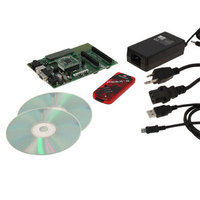
DEVELOPMENT KIT FOR PIC18
Manufacturer
Microchip Technology
Series
PIC®r
Type
MCUr
Datasheets
1.DM183032.pdf
(38 pages)
2.DV164136.pdf
(448 pages)
3.DV164136.pdf
(6 pages)
4.DV164136.pdf
(446 pages)
5.DV164136.pdf
(4 pages)
6.DV164136.pdf
(18 pages)
Specifications of DV164136
Contents
Board, Cables, CDs, PICkit™ 3 Programmer, Power Supply
Processor To Be Evaluated
PIC18F8722, PIC18F87J11
Interface Type
RS-232, USB
Operating Supply Voltage
3.3 V, 5 V
Silicon Manufacturer
Microchip
Core Architecture
PIC
Core Sub-architecture
PIC18
Silicon Core Number
PIC18F
Silicon Family Name
PIC18F8xxx
Kit Contents
PIC18 Exp Brd PICkit 3 Cable CD PSU
Lead Free Status / RoHS Status
Lead free / RoHS Compliant
For Use With/related Products
PIC18F8722, PIC18F87J11
Lead Free Status / Rohs Status
Lead free / RoHS Compliant
Available stocks
Company
Part Number
Manufacturer
Quantity
Price
Company:

Part Number:
DV164136
Manufacturer:
MICROCHIP
Quantity:
12 000


18.4.2
The PWM duty cycle is specified by writing to the
CCPR1L register and to the CCP1CON<5:4> bits. Up
to 10-bit resolution is available. The CCPR1L contains
the eight MSbs and the CCP1CON<5:4> contains the
two LSbs. This 10-bit value is represented by
CCPR1L:CCP1CON<5:4>. The PWM duty cycle is
calculated by the following equation:
EQUATION 18-2:
CCPR1L and CCP1CON<5:4> can be written to at any
time but the duty cycle value is not copied into
CCPR1H until a match between PR2 and TMR2 occurs
(i.e., the period is complete). In PWM mode, CCPR1H
is a read-only register.
The CCPR1H register and a 2-bit internal latch are
used to double-buffer the PWM duty cycle. This
double-buffering is essential for glitchless PWM opera-
tion. When the CCPR1H and 2-bit latch match TMR2,
concatenated with an internal 2-bit Q clock or two bits
of the TMR2 prescaler, the ECCP1 pin is cleared. The
maximum PWM resolution (bits) for a given PWM
frequency is given by the equation:
EQUATION 18-3:
TABLE 18-4:
© 2009 Microchip Technology Inc.
Timer Prescaler (1, 4, 16)
PR2 Value
Maximum Resolution (bits)
PWM Duty Cycle = (CCPR1L:CCP1CON<5:4>) •
PWM Resolution (max) =
PWM Frequency
PWM DUTY CYCLE
EXAMPLE PWM FREQUENCIES AND RESOLUTIONS AT 40 MHz
T
OSC
• (TMR2 Prescale Value)
log
(
log(2)
2.44 kHz
F
F
PWM
FFh
OSC
16
10
)
bits
9.77 kHz
FFh
10
4
PIC18F87J11 FAMILY
39.06 kHz
18.4.3
The P1M1:P1M0 bits in the CCP1CON register allow
one of four configurations:
• Single Output
• Half-Bridge Output
• Full-Bridge Output, Forward mode
• Full-Bridge Output, Reverse mode
The Single Output mode is the standard PWM mode
discussed in Section 18.4 “Enhanced PWM Mode”.
The Half-Bridge and Full-Bridge Output modes are
covered in detail in the sections that follow.
The general relationship of the outputs in all
configurations is summarized in Figure 18-2.
Note:
FFh
10
1
If the PWM duty cycle value is longer than
the PWM period, the ECCP1 pin will not
be cleared.
PWM OUTPUT CONFIGURATIONS
156.25 kHz
3Fh
1
8
312.50 kHz
1Fh
1
7
DS39778D-page 211
416.67 kHz
6.58
17h
1
Related parts for DV164136
Image
Part Number
Description
Manufacturer
Datasheet
Request
R

Part Number:
Description:
Manufacturer:
Microchip Technology Inc.
Datasheet:
Part Number:
Description:
Manufacturer:
Microchip Technology Inc.
Datasheet:
Part Number:
Description:
Manufacturer:
Microchip Technology Inc.
Datasheet:
Part Number:
Description:
Manufacturer:
Microchip Technology Inc.
Datasheet:
Part Number:
Description:
Manufacturer:
Microchip Technology Inc.
Datasheet:
Part Number:
Description:
Manufacturer:
Microchip Technology Inc.
Datasheet:
Part Number:
Description:
Manufacturer:
Microchip Technology Inc.
Datasheet:
Part Number:
Description:
Manufacturer:
Microchip Technology Inc.
Datasheet: