DEMO9S08EL32 Freescale Semiconductor, DEMO9S08EL32 Datasheet - Page 13
DEMO9S08EL32
Manufacturer Part Number
DEMO9S08EL32
Description
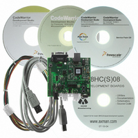
BOARD DEMO FOR 9S08 EL MCU
Manufacturer
Freescale Semiconductor
Type
MCUr
Datasheets
1.DEMO9S08EL32.pdf
(356 pages)
2.DEMO9S08EL32.pdf
(14 pages)
3.DEMO9S08EL32.pdf
(2 pages)
Specifications of DEMO9S08EL32
Contents
Evaluation Board
Processor To Be Evaluated
MC9S08EL32
Data Bus Width
8 bit
Interface Type
RS-232, USB
Operating Supply Voltage
12 V
Silicon Manufacturer
Freescale
Core Architecture
HCS08
Core Sub-architecture
HCS08
Silicon Core Number
MC9S08
Silicon Family Name
S08EL
Rohs Compliant
Yes
For Use With/related Products
MC9S08EL32
Lead Free Status / RoHS Status
Lead free / RoHS Compliant


Section Number
10.4 Functional Description ..................................................................................................................152
10.5 Initialization Information ..............................................................................................................157
10.6 Application Information ................................................................................................................159
11.1 Introduction ...................................................................................................................................165
11.2 External Signal Description ..........................................................................................................168
11.3 Register Definition ........................................................................................................................168
11.4 Functional Description ..................................................................................................................175
11.5 Resets ............................................................................................................................................179
Freescale Semiconductor
10.3.6 Compare Value Low Register (ADCCVL) .....................................................................147
10.3.7 Configuration Register (ADCCFG) ................................................................................147
10.3.8 Pin Control 1 Register (APCTL1) ..................................................................................149
10.3.9 Pin Control 2 Register (APCTL2) ..................................................................................150
10.3.10Pin Control 3 Register (APCTL3) ..................................................................................151
10.4.1 Clock Select and Divide Control ....................................................................................152
10.4.2 Input Select and Pin Control ...........................................................................................153
10.4.3 Hardware Trigger ............................................................................................................153
10.4.4 Conversion Control .........................................................................................................153
10.4.5 Automatic Compare Function .........................................................................................156
10.4.6 MCU Wait Mode Operation ............................................................................................156
10.4.7 MCU Stop3 Mode Operation ..........................................................................................156
10.4.8 MCU Stop1 and Stop2 Mode Operation .........................................................................157
10.5.1 ADC Module Initialization Example .............................................................................157
10.6.1 External Pins and Routing ..............................................................................................159
10.6.2 Sources of Error ..............................................................................................................161
11.1.1 Module Configuration .....................................................................................................165
11.1.2 Features ...........................................................................................................................167
11.1.3 Modes of Operation ........................................................................................................167
11.1.4 Block Diagram ................................................................................................................168
11.2.1 SCL — Serial Clock Line ...............................................................................................168
11.2.2 SDA — Serial Data Line ................................................................................................168
11.3.1 IIC Address Register (IICA) ...........................................................................................169
11.3.2 IIC Frequency Divider Register (IICF) ..........................................................................169
11.3.3 IIC Control Register (IICC1) ..........................................................................................172
11.3.4 IIC Status Register (IICS) ...............................................................................................172
11.3.5 IIC Data I/O Register (IICD) ..........................................................................................173
11.3.6 IIC Control Register 2 (IICC2) .......................................................................................174
11.4.1 IIC Protocol .....................................................................................................................175
11.4.2 10-bit Address .................................................................................................................178
11.4.3 General Call Address ......................................................................................................179
MC9S08EL32 Series and MC9S08SL16 Series Data Sheet, Rev. 3
Inter-Integrated Circuit (S08IICV2)
Chapter 11
Title
Page
13
Related parts for DEMO9S08EL32
Image
Part Number
Description
Manufacturer
Datasheet
Request
R

Part Number:
Description:
Manufacturer:
Freescale Semiconductor, Inc
Datasheet:
Part Number:
Description:
Manufacturer:
Freescale Semiconductor, Inc
Datasheet:
Part Number:
Description:
Manufacturer:
Freescale Semiconductor, Inc
Datasheet:
Part Number:
Description:
Manufacturer:
Freescale Semiconductor, Inc
Datasheet:
Part Number:
Description:
Manufacturer:
Freescale Semiconductor, Inc
Datasheet:
Part Number:
Description:
Manufacturer:
Freescale Semiconductor, Inc
Datasheet:
Part Number:
Description:
Manufacturer:
Freescale Semiconductor, Inc
Datasheet:
Part Number:
Description:
Manufacturer:
Freescale Semiconductor, Inc
Datasheet:
Part Number:
Description:
Manufacturer:
Freescale Semiconductor, Inc
Datasheet:
Part Number:
Description:
Manufacturer:
Freescale Semiconductor, Inc
Datasheet:
Part Number:
Description:
Manufacturer:
Freescale Semiconductor, Inc
Datasheet:
Part Number:
Description:
Manufacturer:
Freescale Semiconductor, Inc
Datasheet:
Part Number:
Description:
Manufacturer:
Freescale Semiconductor, Inc
Datasheet:
Part Number:
Description:
Manufacturer:
Freescale Semiconductor, Inc
Datasheet:
Part Number:
Description:
Manufacturer:
Freescale Semiconductor, Inc
Datasheet: