C8051F800DK Silicon Laboratories Inc, C8051F800DK Datasheet - Page 11
C8051F800DK
Manufacturer Part Number
C8051F800DK
Description
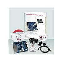
KIT DEV C8051F800
Manufacturer
Silicon Laboratories Inc
Type
MCUr
Specifications of C8051F800DK
Contents
Board, Cables, CD, Debugger, Power Supply
Processor To Be Evaluated
C8051F800
Data Bus Width
16 bit
Interface Type
USB
Operating Supply Voltage
7 V to 15 V
Lead Free Status / RoHS Status
Contains lead / RoHS non-compliant
For Use With/related Products
C8051F8xx
Lead Free Status / Rohs Status
Supplier Unconfirmed
Other names
336-1797


27. UART0
28. Timers
29. Programmable Counter Array
30. C2 Interface
Figure 26.3. SMBus Transaction ........................................................................... 182
Figure 26.4. Typical SMBus SCL Generation ........................................................ 184
Figure 26.5. Typical Master Write Sequence ........................................................ 193
Figure 26.6. Typical Master Read Sequence ........................................................ 194
Figure 26.7. Typical Slave Write Sequence .......................................................... 195
Figure 26.8. Typical Slave Read Sequence .......................................................... 196
Figure 27.1. UART0 Block Diagram ...................................................................... 201
Figure 27.2. UART0 Baud Rate Logic ................................................................... 202
Figure 27.3. UART Interconnect Diagram ............................................................. 203
Figure 27.4. 8-Bit UART Timing Diagram .............................................................. 203
Figure 27.5. 9-Bit UART Timing Diagram .............................................................. 204
Figure 27.6. UART Multi-Processor Mode Interconnect Diagram ......................... 205
Figure 28.1. T0 Mode 0 Block Diagram ................................................................. 212
Figure 28.2. T0 Mode 2 Block Diagram ................................................................. 213
Figure 28.3. T0 Mode 3 Block Diagram ................................................................. 214
Figure 28.4. Timer 2 16-Bit Mode Block Diagram ................................................. 219
Figure 28.5. Timer 2 8-Bit Mode Block Diagram ................................................... 220
Figure 29.1. PCA Block Diagram ........................................................................... 225
Figure 29.2. PCA Counter/Timer Block Diagram ................................................... 226
Figure 29.3. PCA Interrupt Block Diagram ............................................................ 227
Figure 29.4. PCA Capture Mode Diagram ............................................................. 229
Figure 29.5. PCA Software Timer Mode Diagram ................................................. 230
Figure 29.6. PCA High-Speed Output Mode Diagram ........................................... 231
Figure 29.7. PCA Frequency Output Mode ........................................................... 232
Figure 29.8. PCA 8-Bit PWM Mode Diagram ........................................................ 233
Figure 29.9. PCA 9-bit through 15-Bit PWM Mode Diagram ................................. 234
Figure 29.10. PCA 16-Bit PWM Mode ................................................................... 235
Figure 29.11. PCA Module 2 with Watchdog Timer Enabled ................................ 236
Figure 30.1. Typical C2 Pin Sharing ...................................................................... 247
Rev. 1.0
C8051F80x-83x
11
Related parts for C8051F800DK
Image
Part Number
Description
Manufacturer
Datasheet
Request
R

Part Number:
Description:
SMD/C°/SINGLE-ENDED OUTPUT SILICON OSCILLATOR
Manufacturer:
Silicon Laboratories Inc
Part Number:
Description:
Manufacturer:
Silicon Laboratories Inc
Datasheet:
Part Number:
Description:
N/A N/A/SI4010 AES KEYFOB DEMO WITH LCD RX
Manufacturer:
Silicon Laboratories Inc
Datasheet:
Part Number:
Description:
N/A N/A/SI4010 SIMPLIFIED KEY FOB DEMO WITH LED RX
Manufacturer:
Silicon Laboratories Inc
Datasheet:
Part Number:
Description:
N/A/-40 TO 85 OC/EZLINK MODULE; F930/4432 HIGH BAND (REV E/B1)
Manufacturer:
Silicon Laboratories Inc
Part Number:
Description:
EZLink Module; F930/4432 Low Band (rev e/B1)
Manufacturer:
Silicon Laboratories Inc
Part Number:
Description:
I°/4460 10 DBM RADIO TEST CARD 434 MHZ
Manufacturer:
Silicon Laboratories Inc
Part Number:
Description:
I°/4461 14 DBM RADIO TEST CARD 868 MHZ
Manufacturer:
Silicon Laboratories Inc
Part Number:
Description:
I°/4463 20 DBM RFSWITCH RADIO TEST CARD 460 MHZ
Manufacturer:
Silicon Laboratories Inc
Part Number:
Description:
I°/4463 20 DBM RADIO TEST CARD 868 MHZ
Manufacturer:
Silicon Laboratories Inc
Part Number:
Description:
I°/4463 27 DBM RADIO TEST CARD 868 MHZ
Manufacturer:
Silicon Laboratories Inc
Part Number:
Description:
I°/4463 SKYWORKS 30 DBM RADIO TEST CARD 915 MHZ
Manufacturer:
Silicon Laboratories Inc
Part Number:
Description:
N/A N/A/-40 TO 85 OC/4463 RFMD 30 DBM RADIO TEST CARD 915 MHZ
Manufacturer:
Silicon Laboratories Inc
Part Number:
Description:
I°/4463 20 DBM RADIO TEST CARD 169 MHZ
Manufacturer:
Silicon Laboratories Inc