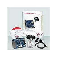
C8051F800DK Silicon Laboratories Inc, C8051F800DK Datasheet - Page 28

C8051F800DK
Manufacturer Part Number
C8051F800DK
Description
KIT DEV C8051F800
Manufacturer
Silicon Laboratories Inc
Type
MCUr
Specifications of C8051F800DK
Contents
Board, Cables, CD, Debugger, Power Supply
Processor To Be Evaluated
C8051F800
Data Bus Width
16 bit
Interface Type
USB
Operating Supply Voltage
7 V to 15 V
Lead Free Status / RoHS Status
Contains lead / RoHS non-compliant
For Use With/related Products
C8051F8xx
Lead Free Status / Rohs Status
Supplier Unconfirmed
Other names
336-1797
- Current page: 28 of 250
- Download datasheet (2Mb)
C8051F80x-83x
3. Pin Definitions
28
XTAL1
XTAL2
Name
C2CK
VREF
P2.0/
P0.0/
P0.2/
P0.3/
GND
RST/
P0.1
P0.4
C2D
V
DD
QSOP-24
Pin
23
22
5
6
7
8
4
3
2
Table 3.1. Pin Definitions for the C8051F80x-83x
QFN-20
Pin
20
19
18
17
2
3
4
5
1
SOIC-16
Pin
16
15
4
5
6
7
3
2
1
D I/O or
D I/O or
D I/O or
D I/O or
D I/O or
A I/O or
Type
D I/O
D I/O
D I/O
D I/O
A In
A In
A In
A In
A In
A In
D In
A In
Rev. 1.0
Description
Ground.
This ground connection is required. The center
pad may optionally be connected to ground as
well on the QFN-20 packages.
Power Supply Voltage.
Device Reset. Open-drain output of internal
POR or V
tiate a system reset by driving this pin low for at
least 10 µs.
Clock signal for the C2 Debug Interface.
Bi-directional data signal for the C2 Debug Inter-
face. Shared with P2.0 on 20-pin packaging and
P2.4 on 24-pin packaging.
Bi-directional data signal for the C2 Debug Inter-
face. Shared with P2.0 on 20-pin packaging and
P2.4 on 24-pin packaging.
Port 0.0.
External VREF input.
Port 0.1.
Port 0.2.
External Clock Input. This pin is the external
oscillator return for a crystal or resonator.
Port 0.3.
External Clock Output. For an external crystal or
resonator, this pin is the excitation driver. This
pin is the external clock input for CMOS, capaci-
tor, or RC oscillator configurations.
Port 0.4.
DD
monitor. An external source can ini-
Related parts for C8051F800DK
Image
Part Number
Description
Manufacturer
Datasheet
Request
R
Part Number:
Description:
SMD/C°/SINGLE-ENDED OUTPUT SILICON OSCILLATOR
Manufacturer:
Silicon Laboratories Inc
Part Number:
Description:
Manufacturer:
Silicon Laboratories Inc
Datasheet:
Part Number:
Description:
N/A N/A/SI4010 AES KEYFOB DEMO WITH LCD RX
Manufacturer:
Silicon Laboratories Inc
Datasheet:
Part Number:
Description:
N/A N/A/SI4010 SIMPLIFIED KEY FOB DEMO WITH LED RX
Manufacturer:
Silicon Laboratories Inc
Datasheet:
Part Number:
Description:
N/A/-40 TO 85 OC/EZLINK MODULE; F930/4432 HIGH BAND (REV E/B1)
Manufacturer:
Silicon Laboratories Inc
Part Number:
Description:
EZLink Module; F930/4432 Low Band (rev e/B1)
Manufacturer:
Silicon Laboratories Inc
Part Number:
Description:
I°/4460 10 DBM RADIO TEST CARD 434 MHZ
Manufacturer:
Silicon Laboratories Inc
Part Number:
Description:
I°/4461 14 DBM RADIO TEST CARD 868 MHZ
Manufacturer:
Silicon Laboratories Inc
Part Number:
Description:
I°/4463 20 DBM RFSWITCH RADIO TEST CARD 460 MHZ
Manufacturer:
Silicon Laboratories Inc
Part Number:
Description:
I°/4463 20 DBM RADIO TEST CARD 868 MHZ
Manufacturer:
Silicon Laboratories Inc
Part Number:
Description:
I°/4463 27 DBM RADIO TEST CARD 868 MHZ
Manufacturer:
Silicon Laboratories Inc
Part Number:
Description:
I°/4463 SKYWORKS 30 DBM RADIO TEST CARD 915 MHZ
Manufacturer:
Silicon Laboratories Inc
Part Number:
Description:
N/A N/A/-40 TO 85 OC/4463 RFMD 30 DBM RADIO TEST CARD 915 MHZ
Manufacturer:
Silicon Laboratories Inc
Part Number:
Description:
I°/4463 20 DBM RADIO TEST CARD 169 MHZ
Manufacturer:
Silicon Laboratories Inc


