HW-V5-ML501-UNI-G Xilinx Inc, HW-V5-ML501-UNI-G Datasheet - Page 18
HW-V5-ML501-UNI-G
Manufacturer Part Number
HW-V5-ML501-UNI-G
Description
EVALUATION PLATFORM VIRTEX-5
Manufacturer
Xilinx Inc
Series
Virtex™-5 LXr
Type
FPGAr
Datasheet
1.HW-V5-ML501-UNI-G.pdf
(42 pages)
Specifications of HW-V5-ML501-UNI-G
Design Resources
ML501 Ref Design User Guide ML501 Schematics
Contents
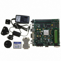
ML501 Platform, DVI Adapter and CompactFlash Card
Silicon Manufacturer
Xilinx
Features
Programmable System Clock Generator Chip, RS-232 Serial Port
Silicon Family Name
Virtex-5
Silicon Core Number
XC5VLX50FFG676
Lead Free Status / RoHS Status
Lead free / RoHS Compliant
For Use With/related Products
XC5VLX50FFG676
Lead Free Status / RoHS Status
Lead free / RoHS Compliant, Lead free / RoHS Compliant
Other names
122-1508
Available stocks
Company
Part Number
Manufacturer
Quantity
Price


Chapter 1: ML501 Evaluation Platform
18
4. Oscillator Sockets
5. LCD Brightness and Contrast Adjustment
6. DIP Switches (Active-High)
The board has one crystal oscillator socket (X1) wired for standard LVTTL-type oscillators.
It connects to the FPGA clock pin as shown in
100-MHz oscillator and is powered by the 3.3V supply.
The board also provides an IDT5V9885 (U8) EEPROM programmable clock generator
device. This device is used to generate a variety of clocks to the board peripherals and
FPGA. The programmable clock generator provides the following factory default single-
ended outputs:
•
•
•
•
•
If users change the factory default configuration of the clock generator chip, the related
reference design material might not work as designed. Instructions for returning the
IDT5V9885 to the factory default configuration are provided in
“Programming the IDT Clock Chip.”
Table 1-4: Oscillator Socket Connection
Turning potentiometer R87 adjusts the image contrast of the character LCD. The
potentiometer should be turned with a screwdriver.
Eight general-purpose (active-High) DIP switches are connected to the user I/O pins of the
FPGA.
Table 1-5: DIP Switch Connections (SW4)
GPIO_DIP_SW1
GPIO_DIP_SW2
GPIO_DIP_SW3
GPIO_DIP_SW4
GPIO_DIP_SW5
Label
25 MHz to the Ethernet PHY (U13)
14.318 MHz to the audio codec (U16)
27 MHz to the USB controller (U18)
33 MHz to the Xilinx System ACE CF (U2)
33 MHz, 27 MHz, and a differential 200 MHz clock to the Xilinx FPGA
U8
U8
U8
U8
X1
Table 1-5
SW4
CLK_DIFF_FPGA_N
CLK_33MHZ_FPGA
CLK_27MHZ_FPGA
CLK_DIFF_FPGA_P
summarizes these connections.
Clock Name
USER_CLK
www.xilinx.com
FPGA Pin
U4
V3
U6
T4
T5
FPGA Pin
AD13
AB12
AD8
E16
E17
Table
1-4. The X1 socket is populated with a
200 MHz differential pair (pos)
100 MHz single-ended
33 MHz single-ended
27 MHz single-ended
200 MHz differential pair (neg)
UG226 (v1.4) August 24, 2009
Description
Appendix A,
ML501 Evaluation Platform
R
Related parts for HW-V5-ML501-UNI-G
Image
Part Number
Description
Manufacturer
Datasheet
Request
R

Part Number:
Description:
IC CPLD .8K 36MCELL 44-VQFP
Manufacturer:
Xilinx Inc
Datasheet:

Part Number:
Description:
IC CPLD 72MCRCELL 10NS 44VQFP
Manufacturer:
Xilinx Inc
Datasheet:

Part Number:
Description:
IC CPLD 1.6K 72MCELL 64-VQFP
Manufacturer:
Xilinx Inc
Datasheet:

Part Number:
Description:
IC CR-II CPLD 64MCELL 44-VQFP
Manufacturer:
Xilinx Inc
Datasheet:

Part Number:
Description:
IC CPLD 1.6K 72MCELL 100-TQFP
Manufacturer:
Xilinx Inc
Datasheet:

Part Number:
Description:
IC CR-II CPLD 64MCELL 56-BGA
Manufacturer:
Xilinx Inc
Datasheet:

Part Number:
Description:
IC CPLD 72MCRCELL 7.5NS 44VQFP
Manufacturer:
Xilinx Inc
Datasheet:
Part Number:
Description:
IC CR-II CPLD 64MCELL 100-VQFP
Manufacturer:
Xilinx Inc
Datasheet:
Part Number:
Description:
IC CPLD 1.6K 72MCELL 100-TQFP
Manufacturer:
Xilinx Inc
Datasheet:

Part Number:
Description:
IC CPLD 72MCRCELL 7.5NS 64VQFP
Manufacturer:
Xilinx Inc
Datasheet:
Part Number:
Description:
IC CPLD 1.6K 72MCELL 100-TQFP
Manufacturer:
Xilinx Inc
Datasheet:

Part Number:
Description:
IC CPLD 1.5K 64MCELL HP 44-VQFP
Manufacturer:
Xilinx Inc

Part Number:
Description:
IC CPLD 36MCRCELL 15NS 44PLCC
Manufacturer:
Xilinx Inc
Datasheet:

Part Number:
Description:
IC CPLD 36MCRCELL 10NS 44PLCC
Manufacturer:
Xilinx Inc
Datasheet:

Part Number:
Description:
IC CPLD 1.5K 64MCELL HP 44-VQFP
Manufacturer:
Xilinx Inc