HW-V5-ML501-UNI-G Xilinx Inc, HW-V5-ML501-UNI-G Datasheet - Page 28
HW-V5-ML501-UNI-G
Manufacturer Part Number
HW-V5-ML501-UNI-G
Description
EVALUATION PLATFORM VIRTEX-5
Manufacturer
Xilinx Inc
Series
Virtex™-5 LXr
Type
FPGAr
Datasheet
1.HW-V5-ML501-UNI-G.pdf
(42 pages)
Specifications of HW-V5-ML501-UNI-G
Design Resources
ML501 Ref Design User Guide ML501 Schematics
Contents
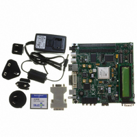
ML501 Platform, DVI Adapter and CompactFlash Card
Silicon Manufacturer
Xilinx
Features
Programmable System Clock Generator Chip, RS-232 Serial Port
Silicon Family Name
Virtex-5
Silicon Core Number
XC5VLX50FFG676
Lead Free Status / RoHS Status
Lead free / RoHS Compliant
For Use With/related Products
XC5VLX50FFG676
Lead Free Status / RoHS Status
Lead free / RoHS Compliant, Lead free / RoHS Compliant
Other names
122-1508
Available stocks
Company
Part Number
Manufacturer
Quantity
Price


Chapter 1: ML501 Evaluation Platform
28
18. ZBT Synchronous SRAM
19. Linear Flash Chips
20. Xilinx XC95144XL CPLD
21. 10/100/1000 Tri-Speed Ethernet PHY
Note:
and Mode DIP Switches.”
The board also features a System ACE failsafe mode. In this mode, if the System ACE
controller detects a failed configuration attempt, it automatically reboots back to a
predefined configuration image. The failsafe mode is enabled by inserting two jumpers
across J18 and J19 (in horizontal or vertical orientation).
The System ACE MPU port is connected to the FPGA. This connection allows the FPGA to
use the System ACE controller to reconfigure the system or access the CompactFlash card
as a generic FAT file system. The data bus for the System ACE MPU port is shared with the
USB controller.
The ZBT synchronous SRAM (ISSI IS61NLP25636A-200TQL) provides high-speed, low-
latency external memory to the FPGA. The memory is organized as 256K x 36 bits. This
organization provides for a 32-bit data bus with support for four parity bits.
Note:
A NOR linear flash device (Intel JS28F256P30T95) is installed on the board to provide
32 MB of flash memory. This memory provides non-volatile storage of data, software, or
bitstreams. The flash chip is 16 bits wide and shares its data bus with SRAM. The flash
memory can also be used to program the FPGA.
Note:
is designed to be asserted at power-on or at system reset.
A Xilinx XC95144XL CPLD provides general-purpose glue logic for the board. The CPLD
is located under the removable LCD and is not visible in
programmed from the main JTAG chain of the board. The CPLD is mainly used to
implement level translators, simple gates, and buffers.
The ML501 Evaluation Platform contains a Marvell Alaska PHY device (88E1111)
operating at 10/100/1000 Mb/s. The board supports MII, GMII, and RGMII interface
modes with the FPGA. The PHY is connected to a Halo HFJ11-1G01E RJ-45 connector with
built-in magnetics. The PHY is configured to default at power-on or reset to the following
Caution!
Improper insertion can cause a short with the traces or components on the board.
System ACE configuration is enabled by way of a DIP switch. See
The SRAM and FLASH memory share the same data bus.
The reset for the AC97 Codec is shared with the reset signal for the flash memory chips and
Use caution when inserting a CompactFlash card with exposed metallic surfaces.
www.xilinx.com
Figure
UG226 (v1.4) August 24, 2009
ML501 Evaluation Platform
1-2. The CPLD is
“31. Configuration Address
R
Related parts for HW-V5-ML501-UNI-G
Image
Part Number
Description
Manufacturer
Datasheet
Request
R

Part Number:
Description:
IC CPLD .8K 36MCELL 44-VQFP
Manufacturer:
Xilinx Inc
Datasheet:

Part Number:
Description:
IC CPLD 72MCRCELL 10NS 44VQFP
Manufacturer:
Xilinx Inc
Datasheet:

Part Number:
Description:
IC CPLD 1.6K 72MCELL 64-VQFP
Manufacturer:
Xilinx Inc
Datasheet:

Part Number:
Description:
IC CR-II CPLD 64MCELL 44-VQFP
Manufacturer:
Xilinx Inc
Datasheet:

Part Number:
Description:
IC CPLD 1.6K 72MCELL 100-TQFP
Manufacturer:
Xilinx Inc
Datasheet:

Part Number:
Description:
IC CR-II CPLD 64MCELL 56-BGA
Manufacturer:
Xilinx Inc
Datasheet:

Part Number:
Description:
IC CPLD 72MCRCELL 7.5NS 44VQFP
Manufacturer:
Xilinx Inc
Datasheet:
Part Number:
Description:
IC CR-II CPLD 64MCELL 100-VQFP
Manufacturer:
Xilinx Inc
Datasheet:
Part Number:
Description:
IC CPLD 1.6K 72MCELL 100-TQFP
Manufacturer:
Xilinx Inc
Datasheet:

Part Number:
Description:
IC CPLD 72MCRCELL 7.5NS 64VQFP
Manufacturer:
Xilinx Inc
Datasheet:
Part Number:
Description:
IC CPLD 1.6K 72MCELL 100-TQFP
Manufacturer:
Xilinx Inc
Datasheet:

Part Number:
Description:
IC CPLD 1.5K 64MCELL HP 44-VQFP
Manufacturer:
Xilinx Inc

Part Number:
Description:
IC CPLD 36MCRCELL 15NS 44PLCC
Manufacturer:
Xilinx Inc
Datasheet:

Part Number:
Description:
IC CPLD 36MCRCELL 10NS 44PLCC
Manufacturer:
Xilinx Inc
Datasheet:

Part Number:
Description:
IC CPLD 1.5K 64MCELL HP 44-VQFP
Manufacturer:
Xilinx Inc