HW-V5-ML501-UNI-G Xilinx Inc, HW-V5-ML501-UNI-G Datasheet - Page 34
HW-V5-ML501-UNI-G
Manufacturer Part Number
HW-V5-ML501-UNI-G
Description
EVALUATION PLATFORM VIRTEX-5
Manufacturer
Xilinx Inc
Series
Virtex™-5 LXr
Type
FPGAr
Datasheet
1.HW-V5-ML501-UNI-G.pdf
(42 pages)
Specifications of HW-V5-ML501-UNI-G
Design Resources
ML501 Ref Design User Guide ML501 Schematics
Contents
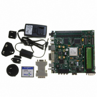
ML501 Platform, DVI Adapter and CompactFlash Card
Silicon Manufacturer
Xilinx
Features
Programmable System Clock Generator Chip, RS-232 Serial Port
Silicon Family Name
Virtex-5
Silicon Core Number
XC5VLX50FFG676
Lead Free Status / RoHS Status
Lead free / RoHS Compliant
For Use With/related Products
XC5VLX50FFG676
Lead Free Status / RoHS Status
Lead free / RoHS Compliant, Lead free / RoHS Compliant
Other names
122-1508
Available stocks
Company
Part Number
Manufacturer
Quantity
Price


Chapter 1: ML501 Evaluation Platform
34
37. System Monitor
The ML501 supports both the dedicated and the auxiliary analog inputs to the Virtex-5
FPGA System Monitor block. The VP and VN pins shown in
dedicated pins, whereas the VAUXP[x], VAUXN[x] represent the 16 user-selectable
auxiliary analog input channels. The ML501 PCB layout for the VP and VN pins is
designed using differential pairs and anti-alias filtering in close proximity to the FPGA as
recommended in the Virtex-5 FPGA System Monitor User Guide
circuitry connected to the 16 AUX channels on the ML501 are connected in a non-optimal
fashion as they are implemented without anti-alias filtering at the FPGA. This tradeoff was
made as the AUX channels are also used as general-purpose I/O on the XGI connectors
(see
still available for use with the System Monitor functions, but they will not attain the
performance level of the dedicated analog input as noted in the Virtex-5 FPGA System
Monitor User Guide. Access to the dedicated analog input pairs (VP/VN) is provided
through pins 9 and 10 of the System Monitor Header (J15). See
The Virtex-5 FPGA System Monitor function is built around a 10-bit, 200-kSPS
(kilosamples per second) Analog-to-Digital Converter (ADC). When combined with a
number of on-chip sensors, the ADC is used to measure FPGA physical operating
parameters like on-chip power supply voltages and die temperatures. Access to external
voltages is provided through a dedicated analog-input pair (VP/VN) and 16 user
selectable analog inputs, known as auxiliary analog inputs (VAUXP[15:0], VAUXN[15:0]).
The System Monitor is fully functional on power up, and measurement data can be
accessed via the JTAG port pre-configuration. The Xilinx
access to the System Monitor over the JTAG port. The System Monitor control logic
implements some common monitoring features. For example, an automatic channel
sequencer allows a user-defined selection of parameters to be automatically monitored,
and user-programmable averaging is enabled to ensure robust noise-free measurements.
The System Monitor also provides user-programmable alarm thresholds for the on-chip
sensors. Thus, if an on-chip monitored parameter moves outside the user-specified
operating range, an alarm logic output becomes active. In addition to monitoring the on-
chip temperature for user-defined applications, the System Monitor issues a special alarm
called Over-Temperature (OT) if the FPGA temperature becomes critical (> 125°C). The
over-temperature signal is deactivated when the device temperature falls below a user-
specified lower limit. If the FPGA power-down feature is enabled, the FPGA enters power
down when the OT signal becomes active. The FPGA powers up again when the alarm is
deactivated.
For additional information about the System Monitor, see
http://www.xilinx.com/systemmonitor
User Guide
Table 1-16: System Monitor Connections
VN
VP
VAUXN[0]
VAUXP[0]
VAUXN[1]
External Input
“10. XGI Expansion Headers,” page 20
[Ref
8].
Table 1-16
FPGA Pin
N14
M24
M26
N24
P13
www.xilinx.com
shows the System Monitor connections.
Header Pin
and consult the Virtex-5 FPGA System Monitor
J15-10
J15-9
J6-30
J6-32
J6-26
for additional details). The AUX channels are
ChipScope™ Pro tool
Schematic Net Name
HDR1_30_SM_0_N
HDR1_26_SM_1_N
HDR1_32_SM_0_P
Table 1-16, page 34
UG226 (v1.4) August 24, 2009
[Ref
Table
FPGA_V_N
FPGA_V_P
ML501 Evaluation Platform
8]. Please note that the
1-16.
provides
are the
R
Related parts for HW-V5-ML501-UNI-G
Image
Part Number
Description
Manufacturer
Datasheet
Request
R

Part Number:
Description:
IC CPLD .8K 36MCELL 44-VQFP
Manufacturer:
Xilinx Inc
Datasheet:

Part Number:
Description:
IC CPLD 72MCRCELL 10NS 44VQFP
Manufacturer:
Xilinx Inc
Datasheet:

Part Number:
Description:
IC CPLD 1.6K 72MCELL 64-VQFP
Manufacturer:
Xilinx Inc
Datasheet:

Part Number:
Description:
IC CR-II CPLD 64MCELL 44-VQFP
Manufacturer:
Xilinx Inc
Datasheet:

Part Number:
Description:
IC CPLD 1.6K 72MCELL 100-TQFP
Manufacturer:
Xilinx Inc
Datasheet:

Part Number:
Description:
IC CR-II CPLD 64MCELL 56-BGA
Manufacturer:
Xilinx Inc
Datasheet:

Part Number:
Description:
IC CPLD 72MCRCELL 7.5NS 44VQFP
Manufacturer:
Xilinx Inc
Datasheet:
Part Number:
Description:
IC CR-II CPLD 64MCELL 100-VQFP
Manufacturer:
Xilinx Inc
Datasheet:
Part Number:
Description:
IC CPLD 1.6K 72MCELL 100-TQFP
Manufacturer:
Xilinx Inc
Datasheet:

Part Number:
Description:
IC CPLD 72MCRCELL 7.5NS 64VQFP
Manufacturer:
Xilinx Inc
Datasheet:
Part Number:
Description:
IC CPLD 1.6K 72MCELL 100-TQFP
Manufacturer:
Xilinx Inc
Datasheet:

Part Number:
Description:
IC CPLD 1.5K 64MCELL HP 44-VQFP
Manufacturer:
Xilinx Inc

Part Number:
Description:
IC CPLD 36MCRCELL 15NS 44PLCC
Manufacturer:
Xilinx Inc
Datasheet:

Part Number:
Description:
IC CPLD 36MCRCELL 10NS 44PLCC
Manufacturer:
Xilinx Inc
Datasheet:

Part Number:
Description:
IC CPLD 1.5K 64MCELL HP 44-VQFP
Manufacturer:
Xilinx Inc