HW-V5-ML501-UNI-G Xilinx Inc, HW-V5-ML501-UNI-G Datasheet - Page 37
HW-V5-ML501-UNI-G
Manufacturer Part Number
HW-V5-ML501-UNI-G
Description
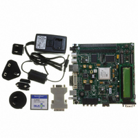
EVALUATION PLATFORM VIRTEX-5
Manufacturer
Xilinx Inc
Series
Virtex™-5 LXr
Type
FPGAr
Datasheet
1.HW-V5-ML501-UNI-G.pdf
(42 pages)
Specifications of HW-V5-ML501-UNI-G
Design Resources
ML501 Ref Design User Guide ML501 Schematics
Contents
ML501 Platform, DVI Adapter and CompactFlash Card
Silicon Manufacturer
Xilinx
Features
Programmable System Clock Generator Chip, RS-232 Serial Port
Silicon Family Name
Virtex-5
Silicon Core Number
XC5VLX50FFG676
Lead Free Status / RoHS Status
Lead free / RoHS Compliant
For Use With/related Products
XC5VLX50FFG676
Lead Free Status / RoHS Status
Lead free / RoHS Compliant, Lead free / RoHS Compliant
Other names
122-1508
Available stocks
Company
Part Number
Manufacturer
Quantity
Price


ML501 Evaluation Platform
UG226 (v1.4) August 24, 2009
Platform Flash PROM Configuration
Linear Flash Memory Configuration
SPI Flash Memory Configuration
R
The Platform Flash PROM can also be used to program the FPGA. The Platform Flash
PROM can hold up to two configuration images (up to four with compression), which are
selectable by the two least significant bits of the configuration address DIP switches.
The board is wired so the Platform Flash PROM can download bitstreams in Master Serial,
Slave Serial, Master SelectMAP (parallel), or Slave SelectMAP (parallel) modes. Using the
iMPACT tool to program the Platform Flash PROM, the user has the option to select which
of the four modes to use for programming the FPGA. The configuration mode DIP
switches on the board must be set to match the programming method being used by the
Platform Flash PROM.
When set correctly, the Platform Flash PROM programs the FPGA upon power-up or
whenever the Prog button is pressed.
Data stored in the linear flash can be used to program the FPGA (BPI mode). Up to four
configuration images can theoretically be supported.
The configuration mode DIP switches on the board must be set to 010 for BPI_up or 011
for BPI_down.
When set correctly, the FPGA is programmed upon power-up or whenever the Prog
button is pressed.
Data stored in SPI can be used to program the FPGA. The configuration mode DIP
switches must be set to 001 for SPI configuration.
When set correctly, the FPGA is programmed upon power-up or whenever the Prog
button is pressed.
www.xilinx.com
Configuration Options
37
Related parts for HW-V5-ML501-UNI-G
Image
Part Number
Description
Manufacturer
Datasheet
Request
R

Part Number:
Description:
IC CPLD .8K 36MCELL 44-VQFP
Manufacturer:
Xilinx Inc
Datasheet:

Part Number:
Description:
IC CPLD 72MCRCELL 10NS 44VQFP
Manufacturer:
Xilinx Inc
Datasheet:

Part Number:
Description:
IC CPLD 1.6K 72MCELL 64-VQFP
Manufacturer:
Xilinx Inc
Datasheet:

Part Number:
Description:
IC CR-II CPLD 64MCELL 44-VQFP
Manufacturer:
Xilinx Inc
Datasheet:

Part Number:
Description:
IC CPLD 1.6K 72MCELL 100-TQFP
Manufacturer:
Xilinx Inc
Datasheet:

Part Number:
Description:
IC CR-II CPLD 64MCELL 56-BGA
Manufacturer:
Xilinx Inc
Datasheet:

Part Number:
Description:
IC CPLD 72MCRCELL 7.5NS 44VQFP
Manufacturer:
Xilinx Inc
Datasheet:
Part Number:
Description:
IC CR-II CPLD 64MCELL 100-VQFP
Manufacturer:
Xilinx Inc
Datasheet:
Part Number:
Description:
IC CPLD 1.6K 72MCELL 100-TQFP
Manufacturer:
Xilinx Inc
Datasheet:

Part Number:
Description:
IC CPLD 72MCRCELL 7.5NS 64VQFP
Manufacturer:
Xilinx Inc
Datasheet:
Part Number:
Description:
IC CPLD 1.6K 72MCELL 100-TQFP
Manufacturer:
Xilinx Inc
Datasheet:

Part Number:
Description:
IC CPLD 1.5K 64MCELL HP 44-VQFP
Manufacturer:
Xilinx Inc

Part Number:
Description:
IC CPLD 36MCRCELL 15NS 44PLCC
Manufacturer:
Xilinx Inc
Datasheet:

Part Number:
Description:
IC CPLD 36MCRCELL 10NS 44PLCC
Manufacturer:
Xilinx Inc
Datasheet:

Part Number:
Description:
IC CPLD 1.5K 64MCELL HP 44-VQFP
Manufacturer:
Xilinx Inc