C8051F540-TB Silicon Laboratories Inc, C8051F540-TB Datasheet - Page 179
C8051F540-TB
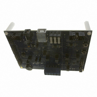
Manufacturer Part Number
C8051F540-TB
Description
BOARD PROTOTYPE W/C8051F540
Manufacturer
Silicon Laboratories Inc
Type
MCUr
Specifications of C8051F540-TB
Contents
Board
Processor To Be Evaluated
C8051F54x
Processor Series
C8051F54x
Interface Type
USB
Operating Supply Voltage
5 V
Lead Free Status / RoHS Status
Lead free / RoHS Compliant
For Use With/related Products
C8051F54x
Lead Free Status / Rohs Status
Lead free / RoHS Compliant
Other names
336-1672


*Note: These registers are used in both master and slave mode. The register bits marked with (m) are accessible only in
LIN0CTRL
LIN0SIZE
LIN0ERR
LIN0MUL
19.7.2. LIN Indirect Access SFR Registers Definitions
Table 19.4 lists the 15 indirect registers used to configured and communicate with the LIN controller.
LIN0DT1
LIN0DT2
LIN0DT3
LIN0DT4
LIN0DT5
LIN0DT6
LIN0DT7
LIN0DT8
LIN0DIV
LIN0ST
LIN0ID
Name
Master mode while the register bits marked with (s) are accessible only in slave mode. All other registers are
accessible in both modes.
Address
0x0A
0x0B
0x0C
0x0D
0x0E
0x00
0x01
0x02
0x03
0x04
0x05
0x06
0x07
0x08
0x09
ENHCHK
STOP(s)
ACTIVE
Table 19.4. LIN Registers* (Indirectly Addressable)
Bit7
PRESCL[1:0]
SLEEP(s)
IDLTOUT ABORT(s) DTREQ(s)
Bit6
TXRX
Bit5
ID5
Rev. 1.1
SYNCH(s) PRTY(s)
DTACK(s)
Bit4
ID4
DIVLSB[7:0]
DATA1[7:0]
DATA2[7:0]
DATA3[7:0]
DATA4[7:0]
DATA5[7:0]
DATA7[7:0]
DATA8[7:0]
DATA67:0]
LINMUL[4:0]
RSTINT RSTERR WUPREQ STREQ(m)
LININT
Bit3
ID3
ERROR
TOUT
Bit2
ID2
LINSIZE[3:0]
C8051F54x
WAKEUP
Bit1
CHK
ID1
BITERR
DONE
DIV9
Bit0
ID0
179
Related parts for C8051F540-TB
Image
Part Number
Description
Manufacturer
Datasheet
Request
R

Part Number:
Description:
SMD/C°/SINGLE-ENDED OUTPUT SILICON OSCILLATOR
Manufacturer:
Silicon Laboratories Inc
Part Number:
Description:
Manufacturer:
Silicon Laboratories Inc
Datasheet:
Part Number:
Description:
N/A N/A/SI4010 AES KEYFOB DEMO WITH LCD RX
Manufacturer:
Silicon Laboratories Inc
Datasheet:
Part Number:
Description:
N/A N/A/SI4010 SIMPLIFIED KEY FOB DEMO WITH LED RX
Manufacturer:
Silicon Laboratories Inc
Datasheet:
Part Number:
Description:
N/A/-40 TO 85 OC/EZLINK MODULE; F930/4432 HIGH BAND (REV E/B1)
Manufacturer:
Silicon Laboratories Inc
Part Number:
Description:
EZLink Module; F930/4432 Low Band (rev e/B1)
Manufacturer:
Silicon Laboratories Inc
Part Number:
Description:
I°/4460 10 DBM RADIO TEST CARD 434 MHZ
Manufacturer:
Silicon Laboratories Inc
Part Number:
Description:
I°/4461 14 DBM RADIO TEST CARD 868 MHZ
Manufacturer:
Silicon Laboratories Inc
Part Number:
Description:
I°/4463 20 DBM RFSWITCH RADIO TEST CARD 460 MHZ
Manufacturer:
Silicon Laboratories Inc
Part Number:
Description:
I°/4463 20 DBM RADIO TEST CARD 868 MHZ
Manufacturer:
Silicon Laboratories Inc
Part Number:
Description:
I°/4463 27 DBM RADIO TEST CARD 868 MHZ
Manufacturer:
Silicon Laboratories Inc
Part Number:
Description:
I°/4463 SKYWORKS 30 DBM RADIO TEST CARD 915 MHZ
Manufacturer:
Silicon Laboratories Inc
Part Number:
Description:
N/A N/A/-40 TO 85 OC/4463 RFMD 30 DBM RADIO TEST CARD 915 MHZ
Manufacturer:
Silicon Laboratories Inc
Part Number:
Description:
I°/4463 20 DBM RADIO TEST CARD 169 MHZ
Manufacturer:
Silicon Laboratories Inc