C8051F540-TB Silicon Laboratories Inc, C8051F540-TB Datasheet - Page 269
C8051F540-TB
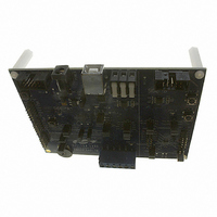
Manufacturer Part Number
C8051F540-TB
Description
BOARD PROTOTYPE W/C8051F540
Manufacturer
Silicon Laboratories Inc
Type
MCUr
Specifications of C8051F540-TB
Contents
Board
Processor To Be Evaluated
C8051F54x
Processor Series
C8051F54x
Interface Type
USB
Operating Supply Voltage
5 V
Lead Free Status / RoHS Status
Lead free / RoHS Compliant
For Use With/related Products
C8051F54x
Lead Free Status / Rohs Status
Lead free / RoHS Compliant
Other names
336-1672


25. C2 Interface
C8051F54x devices include an on-chip Silicon Labs 2-Wire (C2) debug interface to allow Flash program-
ming and in-system debugging with the production part installed in the end application. The C2 interface
uses a clock signal (C2CK) and a bi-directional C2 data signal (C2D) to transfer information between the
device and a host system. See the C2 Interface Specification for details on the C2 protocol.
25.1. C2 Interface Registers
The following describes the C2 registers necessary to perform Flash programming through the C2 inter-
face. All C2 registers are accessed through the C2 interface as described in the C2 Interface Specification.
C2 Register Definition 25.1. C2ADD: C2 Address
Name
Reset
Bit
7:0 C2ADD[7:0] C2 Address.
Type
Bit
Name
7
0
The C2ADD register is accessed via the C2 interface to select the target Data register
for C2 Data Read and Data Write commands.
Address
0x00
0x01
0x02
0xB4
6
0
5
0
Description
Selects the Device ID register for Data Read instructions
Selects the Revision ID register for Data Read instructions
Selects the C2 Flash Programming Control register for Data
Read/Write instructions
Selects the C2 Flash Programming Data register for Data
Read/Write instructions
Rev. 1.1
4
0
C2ADD[7:0]
R/W
Function
3
0
2
0
C8051F54x
1
0
0
0
269
Related parts for C8051F540-TB
Image
Part Number
Description
Manufacturer
Datasheet
Request
R

Part Number:
Description:
SMD/C°/SINGLE-ENDED OUTPUT SILICON OSCILLATOR
Manufacturer:
Silicon Laboratories Inc
Part Number:
Description:
Manufacturer:
Silicon Laboratories Inc
Datasheet:
Part Number:
Description:
N/A N/A/SI4010 AES KEYFOB DEMO WITH LCD RX
Manufacturer:
Silicon Laboratories Inc
Datasheet:
Part Number:
Description:
N/A N/A/SI4010 SIMPLIFIED KEY FOB DEMO WITH LED RX
Manufacturer:
Silicon Laboratories Inc
Datasheet:
Part Number:
Description:
N/A/-40 TO 85 OC/EZLINK MODULE; F930/4432 HIGH BAND (REV E/B1)
Manufacturer:
Silicon Laboratories Inc
Part Number:
Description:
EZLink Module; F930/4432 Low Band (rev e/B1)
Manufacturer:
Silicon Laboratories Inc
Part Number:
Description:
I°/4460 10 DBM RADIO TEST CARD 434 MHZ
Manufacturer:
Silicon Laboratories Inc
Part Number:
Description:
I°/4461 14 DBM RADIO TEST CARD 868 MHZ
Manufacturer:
Silicon Laboratories Inc
Part Number:
Description:
I°/4463 20 DBM RFSWITCH RADIO TEST CARD 460 MHZ
Manufacturer:
Silicon Laboratories Inc
Part Number:
Description:
I°/4463 20 DBM RADIO TEST CARD 868 MHZ
Manufacturer:
Silicon Laboratories Inc
Part Number:
Description:
I°/4463 27 DBM RADIO TEST CARD 868 MHZ
Manufacturer:
Silicon Laboratories Inc
Part Number:
Description:
I°/4463 SKYWORKS 30 DBM RADIO TEST CARD 915 MHZ
Manufacturer:
Silicon Laboratories Inc
Part Number:
Description:
N/A N/A/-40 TO 85 OC/4463 RFMD 30 DBM RADIO TEST CARD 915 MHZ
Manufacturer:
Silicon Laboratories Inc
Part Number:
Description:
I°/4463 20 DBM RADIO TEST CARD 169 MHZ
Manufacturer:
Silicon Laboratories Inc