C8051F540-TB Silicon Laboratories Inc, C8051F540-TB Datasheet - Page 37
C8051F540-TB
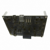
Manufacturer Part Number
C8051F540-TB
Description
BOARD PROTOTYPE W/C8051F540
Manufacturer
Silicon Laboratories Inc
Type
MCUr
Specifications of C8051F540-TB
Contents
Board
Processor To Be Evaluated
C8051F54x
Processor Series
C8051F54x
Interface Type
USB
Operating Supply Voltage
5 V
Lead Free Status / RoHS Status
Lead free / RoHS Compliant
For Use With/related Products
C8051F54x
Lead Free Status / Rohs Status
Lead free / RoHS Compliant
Other names
336-1672


5.3.2. Setting the Gain Value
The three programmable gain registers are accessed indirectly using the ADC0H and ADC0L registers
when the GAINEN bit (ADC0CF.0) bit is set. ADC0H acts as the address register, and ADC0L is the data
register. The programmable gain registers can only be written to and cannot be read. See Gain Register
Definition 5.1, Gain Register Definition 5.2, and Gain Register Definition 5.3 for more information.
The gain is programmed using the following steps:
1. Set the GAINEN bit (ADC0CF.0)
2. Load the ADC0H with the ADC0GNH, ADC0GNL, or ADC0GNA address.
3. Load ADC0L with the desired value for the selected gain register.
4. Reset the GAINEN bit (ADC0CF.0)
Notes:
In code, changing the value to 0.44 gain from the previous example looks like:
// in ‘C’:
ADC0CF |= 0x01;
ADC0H = 0x04;
ADC0L = 0x6C;
ADC0H = 0x07;
ADC0L = 0xA0;
ADC0H = 0x08;
ADC0L = 0x01;
ADC0CF &= ~0x01;
; in assembly
ORL ADC0CF,#01H
MOV ADC0H,#04H
MOV ADC0L,#06CH
MOV ADC0H,#07H
MOV ADC0L,#0A0H
MOV ADC0H,#08H
MOV ADC0L,#01H
ANL ADC0CF,#0FEH
1.
2.
An ADC conversion should not be performed while the GAINEN bit is set
Even with gain enabled, the maximum input voltage must be less than V
voltage of the signal after gain must be less than or equal to V
// GAINEN = 1
// GAINEN = 0
// Load the ADC0GNH address
// Load the upper byte of 0x6CA to ADC0GNH
// Load the ADC0GNL address
// Load the lower nibble of 0x6CA to ADC0GNL
// Load the ADC0GNA address
// Set the GAINADD bit
; GAINEN = 1
; Load the ADC0GNH address
; Load the upper byte of 0x6CA to ADC0GNH
; Load the ADC0GNL address
; Load the lower nibble of 0x6CA to ADC0GNL
; Load the ADC0GNA address
; Set the GAINADD bit
; GAINEN = 0
Rev. 1.1
REF
.
REGIN
.
C8051F54x
and the maximum
37
Related parts for C8051F540-TB
Image
Part Number
Description
Manufacturer
Datasheet
Request
R

Part Number:
Description:
SMD/C°/SINGLE-ENDED OUTPUT SILICON OSCILLATOR
Manufacturer:
Silicon Laboratories Inc
Part Number:
Description:
Manufacturer:
Silicon Laboratories Inc
Datasheet:
Part Number:
Description:
N/A N/A/SI4010 AES KEYFOB DEMO WITH LCD RX
Manufacturer:
Silicon Laboratories Inc
Datasheet:
Part Number:
Description:
N/A N/A/SI4010 SIMPLIFIED KEY FOB DEMO WITH LED RX
Manufacturer:
Silicon Laboratories Inc
Datasheet:
Part Number:
Description:
N/A/-40 TO 85 OC/EZLINK MODULE; F930/4432 HIGH BAND (REV E/B1)
Manufacturer:
Silicon Laboratories Inc
Part Number:
Description:
EZLink Module; F930/4432 Low Band (rev e/B1)
Manufacturer:
Silicon Laboratories Inc
Part Number:
Description:
I°/4460 10 DBM RADIO TEST CARD 434 MHZ
Manufacturer:
Silicon Laboratories Inc
Part Number:
Description:
I°/4461 14 DBM RADIO TEST CARD 868 MHZ
Manufacturer:
Silicon Laboratories Inc
Part Number:
Description:
I°/4463 20 DBM RFSWITCH RADIO TEST CARD 460 MHZ
Manufacturer:
Silicon Laboratories Inc
Part Number:
Description:
I°/4463 20 DBM RADIO TEST CARD 868 MHZ
Manufacturer:
Silicon Laboratories Inc
Part Number:
Description:
I°/4463 27 DBM RADIO TEST CARD 868 MHZ
Manufacturer:
Silicon Laboratories Inc
Part Number:
Description:
I°/4463 SKYWORKS 30 DBM RADIO TEST CARD 915 MHZ
Manufacturer:
Silicon Laboratories Inc
Part Number:
Description:
N/A N/A/-40 TO 85 OC/4463 RFMD 30 DBM RADIO TEST CARD 915 MHZ
Manufacturer:
Silicon Laboratories Inc
Part Number:
Description:
I°/4463 20 DBM RADIO TEST CARD 169 MHZ
Manufacturer:
Silicon Laboratories Inc