EVALPFC1-TDA 4863-2 Infineon Technologies, EVALPFC1-TDA 4863-2 Datasheet - Page 9
EVALPFC1-TDA 4863-2
Manufacturer Part Number
EVALPFC1-TDA 4863-2
Description
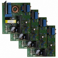
BOARD DEMO 160W DCM-PFC SMPS
Manufacturer
Infineon Technologies
Series
CoolMOS™r
Specifications of EVALPFC1-TDA 4863-2
Main Purpose
Power Management, Power Factor Correction
Embedded
No
Utilized Ic / Part
TDA4863-2
Primary Attributes
160 W, 400 V & 400 mA Out, 85~265 VAC In
Secondary Attributes
Totem Pole Output with Active Shutdown
Lead Free Status / RoHS Status
Lead free / RoHS Compliant
Other names
EVALPFC1-TDA4863-2IN


2
2.1
Conventional electronic ballasts and switch mode power supplies are designed with a
bridge rectifier and a bulk capacitor. Their disadvantage is that the circuit draws power
from the line when the instantaneous AC voltage exceeds the capacitors voltage. This
occurs near the line voltage peak and causes a high charge current spike with following
characteristics: The apparent power is higher than the real power that means low power
factor condition, the current spikes are non sinusoidal with a high content of harmonics
causing line noise, the rectified voltage depends on load condition and requires a large
bulk capacitor, special efforts in noise suppression are necessary.
With the TDA4863-2 preconverter a sinusoidal current is achieved which varies in direct
instantaneous proportional to the input voltage half sine wave and so provides a power
factor near 1. This is due to the appearance of almost any complex load like a resistive
one at the AC line. The harmonic distortions are reduced and comply with the IEC555
standard requirements.
2.2
The TDA4863-2 contains a wide bandwidth voltage amplifier used in a feedback loop,
an overvoltage regulator, an one quadrant multiplier with a wide linear operating range,
a current sense comparator, a zero current detector, a PWM and logic circuitry, a totem-
pole MOSFET driver, an internal trimmed voltage reference, a restart timer and an
undervoltage lockout circuitry.
2.3
With an external capacitor between the pins VSENSE and VAOUT the voltage amplifier
acts like an integrator. The integrator monitors the average output voltage over several
line cycles. Typically the integrator´s bandwidth is set below 20 Hz in order to suppress
the 100 Hz ripple of the rectified line voltage. The voltage amplifier is internally
compensated and has a gain bandwidth of 5 MHz (typ.) and a phase margin of 80
degrees. The non-inverting input is biased internally at 2.5 V. The output is directly
connected to the multiplier input.
The gate drive is disabled when VSENSE voltage is less than 0.2 V or VAOUT voltage
is less than 2.2 V.
If the MOSFET is placed nearby the controller switching interferences have to be taken
into account. The output of the voltage amplifier is designed in a way to minimize these
inteferences.
Version 2.1
Functional Description
Introduction
IC Description
Voltage Amplifier
9
Functional Description
TDA4863-2
22 Feb 2005
Related parts for EVALPFC1-TDA 4863-2
Image
Part Number
Description
Manufacturer
Datasheet
Request
R

Part Number:
Description:
Manufacturer:
Infineon Technologies AG
Datasheet:
Part Number:
Description:
Manufacturer:
Infineon Technologies AG
Datasheet:
Part Number:
Description:
Manufacturer:
Infineon Technologies AG
Datasheet:
Part Number:
Description:
Manufacturer:
Infineon Technologies AG
Datasheet:
Part Number:
Description:
Manufacturer:
Infineon Technologies AG
Datasheet:
Part Number:
Description:
Manufacturer:
Infineon Technologies AG
Datasheet:
Part Number:
Description:
Manufacturer:
Infineon Technologies AG
Datasheet:
Part Number:
Description:
16-bit microcontroller with 2x2 KByte RAM
Manufacturer:
Infineon Technologies AG
Datasheet:
Part Number:
Description:
NPN silicon RF transistor
Manufacturer:
Infineon Technologies AG
Datasheet:
Part Number:
Description:
NPN silicon RF transistor
Manufacturer:
Infineon Technologies AG
Datasheet:
Part Number:
Description:
NPN silicon RF transistor
Manufacturer:
Infineon Technologies AG
Datasheet:
Part Number:
Description:
NPN silicon RF transistor
Manufacturer:
Infineon Technologies AG
Datasheet:
Part Number:
Description:
Si-MMIC-amplifier in SIEGET 25-technologie
Manufacturer:
Infineon Technologies AG
Datasheet:
Part Number:
Description:
IGBT Power Module
Manufacturer:
Infineon Technologies AG
Datasheet:
Part Number:
Description:
IC for switching-mode power supplies
Manufacturer:
Infineon Technologies AG
Datasheet: