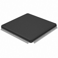
AT32UC3A0128-ALUT Atmel, AT32UC3A0128-ALUT Datasheet - Page 746

AT32UC3A0128-ALUT
Manufacturer Part Number
AT32UC3A0128-ALUT
Description
IC MCU AVR32 128KB FLASH 144LQFP
Manufacturer
Atmel
Series
AVR®32 UC3r
Specifications of AT32UC3A0128-ALUT
Core Processor
AVR
Core Size
32-Bit
Speed
66MHz
Connectivity
EBI/EMI, Ethernet, I²C, SPI, SSC, UART/USART, USB OTG
Peripherals
Brown-out Detect/Reset, POR, PWM, WDT
Number Of I /o
109
Program Memory Size
128KB (128K x 8)
Program Memory Type
FLASH
Ram Size
32K x 8
Voltage - Supply (vcc/vdd)
1.65 V ~ 1.95 V
Data Converters
A/D 8x10b
Oscillator Type
Internal
Operating Temperature
-40°C ~ 85°C
Package / Case
144-LQFP
Processor Series
AT32UC3x
Core
AVR32
Data Bus Width
32 bit
Data Ram Size
32 KB
Interface Type
2-Wire, RS-485, SPI, USART
Maximum Clock Frequency
66 MHz
Number Of Programmable I/os
69
Number Of Timers
3
Maximum Operating Temperature
+ 85 C
Mounting Style
SMD/SMT
3rd Party Development Tools
EWAVR32, EWAVR32-BL, KSK-EVK1100-PL
Development Tools By Supplier
ATAVRDRAGON, ATSTK500, ATSTK600, ATAVRISP2, ATAVRONEKIT, ATEXTWIFI, ATEVK1100, ATEVK1105
Minimum Operating Temperature
- 40 C
Controller Family/series
AT32UC3A
No. Of I/o's
109
Ram Memory Size
32KB
Cpu Speed
66MHz
No. Of Timers
1
Rohs Compliant
Yes
For Use With
ATEVK1105 - KIT EVAL FOR AT32UC3A0ATAVRONEKIT - KIT AVR/AVR32 DEBUGGER/PROGRMMR770-1008 - ISP 4PORT ATMEL AVR32 MCU SPIATEVK1100 - KIT DEV/EVAL FOR AVR32 AT32UC3A
Lead Free Status / RoHS Status
Lead free / RoHS Compliant
Eeprom Size
-
Lead Free Status / Rohs Status
Lead free / RoHS Compliant
Available stocks
Company
Part Number
Manufacturer
Quantity
Price
Company:
Part Number:
AT32UC3A0128-ALUT
Manufacturer:
Atmel
Quantity:
166
- Current page: 746 of 826
- Download datasheet (20Mb)
36.6.4
36.6.4.1
32058J–AVR32–04/11
Service Access Bus
Busy reporting
instruction for the first time. SAMPLE/PRELOAD can also be used for taking a snapshot of the
external pins during normal operation of the part.
When using the JTAG interface for Boundary-Scan, the JTAG TCK clock is independent of the
internal chip clock, which is not required to run.
A number of private instructions are used to access Service Access Bus (SAB) resources. Each
of these are described in detail in SAB address map in the Service Access Bus chapter. The
MEMORY_SIZED_ACCESS instruction allows a sized read or write to any 36-bit address on the
bus. MEMORY_WORD_ACCESS is a shorthand instruction for 32-bit accesses to any 36-bit
address, while the NEXUS_ACCESS instruction is a Nexus-compliant shorthand instruction for
accessing the 32-bit OCD registers in the 7-bit address space reserved for these. These instruc-
tions require two passes through the Shift-DR TAP state: one for the address and control
information, and one for data.
To increase the transfer rate, consecutive memory accesses can be accomplished by the
MEMORY_BLOCK_ACCESS instruction, which only requires a single pass through Shift-DR for
data transfer only. The address is automatically incremented according to the size of the last
SAB transfer.
The access time to SAB resources depends on the type of resource being accessed. It is possi-
ble to read external memory through the EBI, in which case the latency may be very long. It is
possible to abort an ongoing SAB access by the CANCEL_ACCESS instruction, to avoid hang-
ing the bus due to an extremely slow slave.
"The access time to SAB resources depends on the type of resource being
accessed. It is possible to abort an ongoing SAB access by the
CANCEL_ACCESS instruction, to avoid hanging the bus due to an extremely
slow slave."
As the time taken to perform an access may vary depending on system activity and current chip
frequency, all the SAB access JTAG instructions can return a busy indicator. This indicates
whether a delay needs to be inserted, or an operation needs to be repeated in order to be suc-
cessful. If a new access is requested while the SAB is busy, the request is ignored.
The SAB becomes busy when:
The SAB becomes ready again when:
• Entering Update-DR in the address phase of any read operation, e.g. after scanning in a
• Entering Update-DR in the data phase of any write operation, e.g. after scanning in data for a
• Entering Update-DR during a MEMORY_BLOCK_ACCESS.
• Entering Update-DR after scanning in a counter value for SYNC.
• Entering Update-IR after scanning in a MEMORY_BLOCK_ACCESS if the previous access
• A read or write operation completes.
NEXUS_ACCESS address with the read bit set.
NEXUS_ACCESS write.
was a read and data was scanned after scanning the address.
AT32UC3A
746
Related parts for AT32UC3A0128-ALUT
Image
Part Number
Description
Manufacturer
Datasheet
Request
R

Part Number:
Description:
DEV KIT FOR AVR/AVR32
Manufacturer:
Atmel
Datasheet:

Part Number:
Description:
INTERVAL AND WIPE/WASH WIPER CONTROL IC WITH DELAY
Manufacturer:
ATMEL Corporation
Datasheet:

Part Number:
Description:
Low-Voltage Voice-Switched IC for Hands-Free Operation
Manufacturer:
ATMEL Corporation
Datasheet:

Part Number:
Description:
MONOLITHIC INTEGRATED FEATUREPHONE CIRCUIT
Manufacturer:
ATMEL Corporation
Datasheet:

Part Number:
Description:
AM-FM Receiver IC U4255BM-M
Manufacturer:
ATMEL Corporation
Datasheet:

Part Number:
Description:
Monolithic Integrated Feature Phone Circuit
Manufacturer:
ATMEL Corporation
Datasheet:

Part Number:
Description:
Multistandard Video-IF and Quasi Parallel Sound Processing
Manufacturer:
ATMEL Corporation
Datasheet:

Part Number:
Description:
High-performance EE PLD
Manufacturer:
ATMEL Corporation
Datasheet:

Part Number:
Description:
8-bit Flash Microcontroller
Manufacturer:
ATMEL Corporation
Datasheet:

Part Number:
Description:
2-Wire Serial EEPROM
Manufacturer:
ATMEL Corporation
Datasheet:


