ST7FLIT15BY1M6 STMicroelectronics, ST7FLIT15BY1M6 Datasheet - Page 100
ST7FLIT15BY1M6
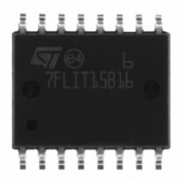
Manufacturer Part Number
ST7FLIT15BY1M6
Description
IC MCU 8BIT 4K FLASH 16-SOIC
Manufacturer
STMicroelectronics
Series
ST7r
Datasheet
1.ST7FLIT15BY1M6.pdf
(159 pages)
Specifications of ST7FLIT15BY1M6
Core Processor
ST7
Core Size
8-Bit
Speed
8MHz
Connectivity
SPI
Peripherals
LVD, POR, PWM, WDT
Number Of I /o
11
Program Memory Size
4KB (4K x 8)
Program Memory Type
FLASH
Ram Size
256 x 8
Voltage - Supply (vcc/vdd)
2.7 V ~ 5.5 V
Data Converters
A/D 7x10b
Oscillator Type
Internal
Operating Temperature
-40°C ~ 85°C
Package / Case
16-SOIC (0.300", 7.5mm Width)
Controller Family/series
ST7
No. Of I/o's
13
Ram Memory Size
256Byte
Cpu Speed
8MHz
No. Of Timers
5
Rohs Compliant
Yes
Processor Series
ST7FLIT1x
Core
ST7
Data Bus Width
8 bit
Data Ram Size
256 B
Interface Type
SPI
Maximum Clock Frequency
8 MHz
Number Of Programmable I/os
17
Number Of Timers
4
Maximum Operating Temperature
+ 85 C
Mounting Style
SMD/SMT
Development Tools By Supplier
ST7FLITE-SK/RAIS, ST7MDT10-DVP3, ST7MDT10-EMU3, STX-RLINK
Minimum Operating Temperature
- 40 C
On-chip Adc
10 bit, 7 Channel
For Use With
497-5049 - KIT STARTER RAISONANCE ST7FLITE497-5046 - KIT TOOL FOR ST7/UPSD/STR7 MCU
Lead Free Status / RoHS Status
Lead free / RoHS Compliant
Eeprom Size
-
Lead Free Status / Rohs Status
Details
Other names
497-8245-5
ST7FLIT15BY1M6
ST7FLIT15BY1M6
Available stocks
Company
Part Number
Manufacturer
Quantity
Price


ST7LITE1xB
11.6 ANALOG COMPARATOR (CMP)
11.6.1 Introduction
The CMP block consists of an analog comparator
and an internal voltage reference. The voltage ref-
erence can be external or internal, selectable un-
der program control. The comparator input pins
COMPIN+ and COMPIN- are also connected to
the A/D converter (ADC).
11.6.2 Main Features
11.6.2.1 On-chip Analog Comparator
The analog comparator compares the voltage at
two input pins COMPIN+ and COMPIN- which are
connected to VP and VN at the comparator input.
When the analog input at COMPIN+ is less than
the analog input at COMPIN-, the output of the
comparator is 0. When the analog input at
COMPIN+ is greater than the analog input at
COMPIN-, the output of the comparator is 1.
The result of the comparison as 0 or 1 at COM-
POUT is shown in
Note:
To obtain a stable result, the comparator requires
a stabilization time of 500ns. Please refer to
tion 13.12 on page
Table 19. Comparison Result
11.6.2.2
Voltage Reference
The voltage reference module can be configured
to connect the comparator pin COMPIN- to one of
the following:
-
-
-
1) Fixed Internal Voltage Bandgap
2) Programmable Internal Voltage Reference
100/159
The voltage reference module can generate a
fixed voltage reference of 1.2V on the VN input.
This is done by setting the VCBGR bit in the
VREFCR register.
Fixed internal voltage bandgap
Programmable internal reference voltage
External voltage reference
CINV
0
1
Programmable
Input Conditions
VP > VN
VN > VP
VP > VN
VN > VP
Figure 62 on page
143.
External/Internal
COMPOUT
101.
0
1
1
0
sec-
3) External Reference Voltage
11.6.3 Functional Description
To make an analog comparison, the CMPON bit in
the CMPCR register must be set to power-on the
comparator and internal voltage reference mod-
ule.
The VP comparator input is mapped on PB0 and is
also connected to ADC channel 0.
The VN comparator input is mapped on PB4 for
external voltage input, and is also connected to
ADC channel 4.
The internal voltage reference can provide a range
of different voltages to the comparator VN input,
selected by several bits in the VREFCR register,
as described in
To select pins PB0 and PB4 for A/D conversion,
(default reset state), channel 0 or 4 must be select-
ed through the channel selection bits in the ADCC-
SR register (refer to
The comparator output is connected to pin PA7
when the COUT bit in the CMPCR register is set.
The comparator output is also connected internally
to the break function of the 12-bit Autoreload Tim-
er (refer to
When the Comparator is OFF, the output value of
comparator is ‘1’.
Important note: To avoid spurious toggling of the
output of the comparator due to noise on the volt-
age reference, it is recommended to enable the
hysteresis through the CHYST bit in the CMPCR
register.
The internal voltage reference module can pro-
vide 16 distinct internally generated voltage lev-
els from 3.2V to 0.2V each at a step of 0.2V on
comparator pin VN. The voltage is selected
through the VR[3:0] bits in the VREFCR regis-
ter.
If a reference voltage other than that generated
by the internal voltage reference module is
required, COMPIN- can be connected to an
external voltage source. This configuration can
be selected by setting the VCEXT bit in the
VREFCR register.
Section
Table
11.2)
Section
20.
11.5.6)
Related parts for ST7FLIT15BY1M6
Image
Part Number
Description
Manufacturer
Datasheet
Request
R

Part Number:
Description:
STMicroelectronics [RIPPLE-CARRY BINARY COUNTER/DIVIDERS]
Manufacturer:
STMicroelectronics
Datasheet:
Part Number:
Description:
STMicroelectronics [LIQUID-CRYSTAL DISPLAY DRIVERS]
Manufacturer:
STMicroelectronics
Datasheet:

Part Number:
Description:
BOARD EVAL FOR MEMS SENSORS
Manufacturer:
STMicroelectronics
Datasheet:
Part Number:
Description:
NPN TRANSISTOR POWER MODULE
Manufacturer:
STMicroelectronics
Datasheet:
Part Number:
Description:
TURBOSWITCH ULTRA-FAST HIGH VOLTAGE DIODE
Manufacturer:
STMicroelectronics
Datasheet:
Part Number:
Description:
Manufacturer:
STMicroelectronics
Datasheet:
Part Number:
Description:
DIODE / SCR MODULE
Manufacturer:
STMicroelectronics
Datasheet:
Part Number:
Description:
DIODE / SCR MODULE
Manufacturer:
STMicroelectronics
Datasheet:
Part Number:
Description:
Search -----> STE16N100
Manufacturer:
STMicroelectronics
Datasheet:
Part Number:
Description:
Search ---> STE53NA50
Manufacturer:
STMicroelectronics
Datasheet:
Part Number:
Description:
NPN Transistor Power Module
Manufacturer:
STMicroelectronics
Datasheet:
Part Number:
Description:
DIODE / SCR MODULE
Manufacturer:
STMicroelectronics
Datasheet: