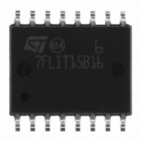
ST7FLIT15BY1M6 STMicroelectronics, ST7FLIT15BY1M6 Datasheet - Page 30

ST7FLIT15BY1M6
Manufacturer Part Number
ST7FLIT15BY1M6
Description
IC MCU 8BIT 4K FLASH 16-SOIC
Manufacturer
STMicroelectronics
Series
ST7r
Datasheet
1.ST7FLIT15BY1M6.pdf
(159 pages)
Specifications of ST7FLIT15BY1M6
Core Processor
ST7
Core Size
8-Bit
Speed
8MHz
Connectivity
SPI
Peripherals
LVD, POR, PWM, WDT
Number Of I /o
11
Program Memory Size
4KB (4K x 8)
Program Memory Type
FLASH
Ram Size
256 x 8
Voltage - Supply (vcc/vdd)
2.7 V ~ 5.5 V
Data Converters
A/D 7x10b
Oscillator Type
Internal
Operating Temperature
-40°C ~ 85°C
Package / Case
16-SOIC (0.300", 7.5mm Width)
Controller Family/series
ST7
No. Of I/o's
13
Ram Memory Size
256Byte
Cpu Speed
8MHz
No. Of Timers
5
Rohs Compliant
Yes
Processor Series
ST7FLIT1x
Core
ST7
Data Bus Width
8 bit
Data Ram Size
256 B
Interface Type
SPI
Maximum Clock Frequency
8 MHz
Number Of Programmable I/os
17
Number Of Timers
4
Maximum Operating Temperature
+ 85 C
Mounting Style
SMD/SMT
Development Tools By Supplier
ST7FLITE-SK/RAIS, ST7MDT10-DVP3, ST7MDT10-EMU3, STX-RLINK
Minimum Operating Temperature
- 40 C
On-chip Adc
10 bit, 7 Channel
For Use With
497-5049 - KIT STARTER RAISONANCE ST7FLITE497-5046 - KIT TOOL FOR ST7/UPSD/STR7 MCU
Lead Free Status / RoHS Status
Lead free / RoHS Compliant
Eeprom Size
-
Lead Free Status / Rohs Status
Details
Other names
497-8245-5
ST7FLIT15BY1M6
ST7FLIT15BY1M6
Available stocks
Company
Part Number
Manufacturer
Quantity
Price
ST7LITE1xB
RESET SEQUENCE MANAGER (Cont’d)
The RESET pin is an asynchronous signal which
plays a major role in EMS performance. In a noisy
environment, it is recommended to follow the
guidelines mentioned in the electrical characteris-
tics section.
7.5.3 External Power-On RESET
If the LVD is disabled by option byte, to start up the
microcontroller correctly, the user must ensure by
means of an external reset circuit that the reset
signal is held low until V
level specified for the selected f
A proper reset signal for a slow rising V
can generally be provided by an external RC net-
work connected to the RESET pin.
Figure 17. RESET Sequences
30/159
1
WATCHDOG
RESET
EXTERNAL
RESET
SOURCE
RESET PIN
V
V
IT+(LVD)
IT-(LVD)
V
RUN
DD
ACTIVE PHASE
DD
RESET
LVD
is over the minimum
OSC
frequency.
DD
RUN
t
h(RSTL)in
supply
WATCHDOG UNDERFLOW
ACTIVE
PHASE
EXTERNAL
RESET
7.5.4 Internal Low Voltage Detector (LVD)
RESET
Two different RESET sequences caused by the in-
ternal LVD circuitry can be distinguished:
■
■
The device RESET pin acts as an output that is
pulled low when V
V
The LVD filters spikes on V
avoid parasitic resets.
7.5.5 Internal Watchdog RESET
The RESET sequence generated by a internal
Watchdog counter overflow is shown in
Starting from the Watchdog counter underflow, the
device RESET pin acts as an output that is pulled
low during at least t
DD
Power-On RESET
Voltage Drop RESET
<V
IT-
INTERNAL RESET (256 or 4096 T
VECTOR FETCH
(falling edge) as shown in
RUN
ACTIVE
PHASE
WATCHDOG
RESET
t
w(RSTL)out
w(RSTL)out
DD
<V
DD
IT+
RUN
.
larger than t
CPU
(rising edge) or
)
Figure
Figure
g(VDD)
17.
17.
to


