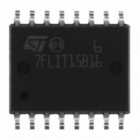
ST7FLIT15BY1M6 STMicroelectronics, ST7FLIT15BY1M6 Datasheet - Page 136

ST7FLIT15BY1M6
Manufacturer Part Number
ST7FLIT15BY1M6
Description
IC MCU 8BIT 4K FLASH 16-SOIC
Manufacturer
STMicroelectronics
Series
ST7r
Datasheet
1.ST7FLIT15BY1M6.pdf
(159 pages)
Specifications of ST7FLIT15BY1M6
Core Processor
ST7
Core Size
8-Bit
Speed
8MHz
Connectivity
SPI
Peripherals
LVD, POR, PWM, WDT
Number Of I /o
11
Program Memory Size
4KB (4K x 8)
Program Memory Type
FLASH
Ram Size
256 x 8
Voltage - Supply (vcc/vdd)
2.7 V ~ 5.5 V
Data Converters
A/D 7x10b
Oscillator Type
Internal
Operating Temperature
-40°C ~ 85°C
Package / Case
16-SOIC (0.300", 7.5mm Width)
Controller Family/series
ST7
No. Of I/o's
13
Ram Memory Size
256Byte
Cpu Speed
8MHz
No. Of Timers
5
Rohs Compliant
Yes
Processor Series
ST7FLIT1x
Core
ST7
Data Bus Width
8 bit
Data Ram Size
256 B
Interface Type
SPI
Maximum Clock Frequency
8 MHz
Number Of Programmable I/os
17
Number Of Timers
4
Maximum Operating Temperature
+ 85 C
Mounting Style
SMD/SMT
Development Tools By Supplier
ST7FLITE-SK/RAIS, ST7MDT10-DVP3, ST7MDT10-EMU3, STX-RLINK
Minimum Operating Temperature
- 40 C
On-chip Adc
10 bit, 7 Channel
For Use With
497-5049 - KIT STARTER RAISONANCE ST7FLITE497-5046 - KIT TOOL FOR ST7/UPSD/STR7 MCU
Lead Free Status / RoHS Status
Lead free / RoHS Compliant
Eeprom Size
-
Lead Free Status / Rohs Status
Details
Other names
497-8245-5
ST7FLIT15BY1M6
ST7FLIT15BY1M6
Available stocks
Company
Part Number
Manufacturer
Quantity
Price
ST7LITE1xB
CONTROL PIN CHARACTERISTICS (Cont’d)
Figure 105. RESET pin protection when LVD is enabled.
Figure 106. RESET pin protection when LVD is disabled.
Note 1:
Note 2: When the LVD is enabled, it is recommended not to connect a pull-up resistor or capacitor. A 10nF pull-down
capacitor is required to filter noise on the reset line.
Note 3: In case a capacitive power supply is used, it is recommended to connect a 1MΩ pull-down resistor to the RESET
pin to discharge any residual voltage induced by the capacitive effect of the power supply (this will add 5µA to the power
consumption of the MCU).
Note 4: Tips when using the LVD:
Note 5: Please refer to “Illegal Opcode Reset” on page 107 for more details on illegal opcode reset conditions.
136/159
– The reset network protects the device against parasitic resets.
– The output of the external reset circuit must have an open-drain output to drive the ST7 reset pad. Otherwise the
– Whatever the reset source is (internal or external), the user must ensure that the level on the RESET pin can go
– Because the reset circuit is designed to allow the internal RESET to be output in the RESET pin, the user must en-
– 1. Check that all recommendations related to ICCCLK and reset circuit have been applied (see caution in Table 1
– 2. Check that the power supply is properly decoupled (100nF + 10µF close to the MCU). Refer to AN1709 and
– 3. The capacitors connected on the RESET pin and also the power supply are key to avoid any start-up marginality.
EXTERNAL
device can be damaged when the ST7 generates an internal reset (LVD or watchdog).
below the V
internally.
sure that the current sunk on the RESET pin is less than the absolute maximum value specified for I
section 13.2.2 on page
on page 7 and notes above)
AN2017. If this cannot be done, it is recommended to put a 100nF + 1MΩ pull-down on the RESET pin.
In most cases, steps 1 and 2 above are sufficient for a robust solution. Otherwise: replace 10nF pull-down on the
RESET pin with a 5µF to 20µF capacitor.”
RESET
Required
EXTERNAL
CIRCUIT
RESET
USER
Required
IL
max. level specified in
0.01μF
111.
0.01μF
1MΩ
Optional
(note 3)
section 13.9.1 on page
V
V
DD
DD
R
R
ON
ON
Filter
Filter
135. Otherwise the reset will not be taken into account
GENERATOR
1)2)3)4)
1)
PULSE
GENERATOR
PULSE
WATCHDOG
WATCHDOG
ILLEGAL OPCODE
LVD RESET
ILLEGAL OPCODE
INTERNAL
RESET
INTERNAL
RESET
INJ(RESET)
ST72XXX
ST72XXX
5)
5)
in


