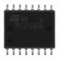
ST7FLIT15BY1M6 STMicroelectronics, ST7FLIT15BY1M6 Datasheet - Page 14

ST7FLIT15BY1M6
Manufacturer Part Number
ST7FLIT15BY1M6
Description
IC MCU 8BIT 4K FLASH 16-SOIC
Manufacturer
STMicroelectronics
Series
ST7r
Datasheet
1.ST7FLIT15BY1M6.pdf
(159 pages)
Specifications of ST7FLIT15BY1M6
Core Processor
ST7
Core Size
8-Bit
Speed
8MHz
Connectivity
SPI
Peripherals
LVD, POR, PWM, WDT
Number Of I /o
11
Program Memory Size
4KB (4K x 8)
Program Memory Type
FLASH
Ram Size
256 x 8
Voltage - Supply (vcc/vdd)
2.7 V ~ 5.5 V
Data Converters
A/D 7x10b
Oscillator Type
Internal
Operating Temperature
-40°C ~ 85°C
Package / Case
16-SOIC (0.300", 7.5mm Width)
Controller Family/series
ST7
No. Of I/o's
13
Ram Memory Size
256Byte
Cpu Speed
8MHz
No. Of Timers
5
Rohs Compliant
Yes
Processor Series
ST7FLIT1x
Core
ST7
Data Bus Width
8 bit
Data Ram Size
256 B
Interface Type
SPI
Maximum Clock Frequency
8 MHz
Number Of Programmable I/os
17
Number Of Timers
4
Maximum Operating Temperature
+ 85 C
Mounting Style
SMD/SMT
Development Tools By Supplier
ST7FLITE-SK/RAIS, ST7MDT10-DVP3, ST7MDT10-EMU3, STX-RLINK
Minimum Operating Temperature
- 40 C
On-chip Adc
10 bit, 7 Channel
For Use With
497-5049 - KIT STARTER RAISONANCE ST7FLITE497-5046 - KIT TOOL FOR ST7/UPSD/STR7 MCU
Lead Free Status / RoHS Status
Lead free / RoHS Compliant
Eeprom Size
-
Lead Free Status / Rohs Status
Details
Other names
497-8245-5
ST7FLIT15BY1M6
ST7FLIT15BY1M6
Available stocks
Company
Part Number
Manufacturer
Quantity
Price
ST7LITE1xB
FLASH PROGRAM MEMORY (Cont’d)
4.5 Memory Protection
There are two different types of memory protec-
tion: Read Out Protection and Write/Erase Protec-
tion which can be applied individually.
4.5.1 Read out Protection
Readout protection, when selected provides a pro-
tection against program memory content extrac-
tion and against write access to Flash memory.
Even if no protection can be considered as totally
unbreakable, the feature provides a very high level
of protection for a general purpose microcontroller.
Both program and data E
In flash devices, this protection is removed by re-
programming the option. In this case, both pro-
gram and data E
erased and the device can be reprogrammed.
Read-out protection selection depends on the de-
vice type:
– In Flash devices it is enabled and removed
– In ROM devices it is enabled by mask option
4.5.2 Flash Write/Erase Protection
Write/erase protection, when set, makes it impos-
sible to both overwrite and erase program memo-
ry. It does not apply to E
provide advanced security to applications and pre-
vent any change being made to the memory con-
tent.
14/159
1
through the FMP_R bit in the option byte.
specified in the Option List.
2
memory are automatically
2
2
memory are protected.
data. Its purpose is to
Warning: Once set, Write/erase protection can
never be removed. A write-protected flash device
is no longer reprogrammable.
Write/erase protection is enabled through the
FMP_W bit in the option byte.
4.6 Related Documentation
For details on Flash programming and ICC proto-
col, refer to the ST7 Flash Programming Refer-
ence Manual and to the ST7 ICC Protocol Refer-
ence Manual
4.7 Register Description
FLASH CONTROL/STATUS REGISTER (FCSR)
Read/Write
Reset Value: 000 0000 (00h)
1st RASS Key: 0101 0110 (56h)
2nd RASS Key: 1010 1110 (AEh)
Note: This register is reserved for programming
using ICP, IAP or other programming methods. It
controls the XFlash programming and erasing op-
erations.
When an EPB or another programming tool is
used (in socket or ICP mode), the RASS keys are
sent automatically.
7
0
0
.
0
0
0
OPT
LAT
PGM
0


