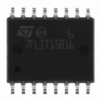
ST7FLIT15BY1M6 STMicroelectronics, ST7FLIT15BY1M6 Datasheet - Page 8

ST7FLIT15BY1M6
Manufacturer Part Number
ST7FLIT15BY1M6
Description
IC MCU 8BIT 4K FLASH 16-SOIC
Manufacturer
STMicroelectronics
Series
ST7r
Datasheet
1.ST7FLIT15BY1M6.pdf
(159 pages)
Specifications of ST7FLIT15BY1M6
Core Processor
ST7
Core Size
8-Bit
Speed
8MHz
Connectivity
SPI
Peripherals
LVD, POR, PWM, WDT
Number Of I /o
11
Program Memory Size
4KB (4K x 8)
Program Memory Type
FLASH
Ram Size
256 x 8
Voltage - Supply (vcc/vdd)
2.7 V ~ 5.5 V
Data Converters
A/D 7x10b
Oscillator Type
Internal
Operating Temperature
-40°C ~ 85°C
Package / Case
16-SOIC (0.300", 7.5mm Width)
Controller Family/series
ST7
No. Of I/o's
13
Ram Memory Size
256Byte
Cpu Speed
8MHz
No. Of Timers
5
Rohs Compliant
Yes
Processor Series
ST7FLIT1x
Core
ST7
Data Bus Width
8 bit
Data Ram Size
256 B
Interface Type
SPI
Maximum Clock Frequency
8 MHz
Number Of Programmable I/os
17
Number Of Timers
4
Maximum Operating Temperature
+ 85 C
Mounting Style
SMD/SMT
Development Tools By Supplier
ST7FLITE-SK/RAIS, ST7MDT10-DVP3, ST7MDT10-EMU3, STX-RLINK
Minimum Operating Temperature
- 40 C
On-chip Adc
10 bit, 7 Channel
For Use With
497-5049 - KIT STARTER RAISONANCE ST7FLITE497-5046 - KIT TOOL FOR ST7/UPSD/STR7 MCU
Lead Free Status / RoHS Status
Lead free / RoHS Compliant
Eeprom Size
-
Lead Free Status / Rohs Status
Details
Other names
497-8245-5
ST7FLIT15BY1M6
ST7FLIT15BY1M6
Available stocks
Company
Part Number
Manufacturer
Quantity
Price
ST7LITE1xB
Notes:
1. It is mandatory to connect all available V
pins to ground.
2. When the pin is configured as analog input, positive and negative current injections are not allowed.
3. PCOR not implemented but p-transistor always active in output mode (refer to
8/159
1
12 10 10
13 11 11
14 12 12 PA4/ATPWM2
15 13
16 14 13 PA2/ATPWM0
17 15
18 16 14 PA0/LTIC
19 17 15 OSC2/PC1
20 18 16 OSC1/CLKIN/PC0 I/O
Pin No.
-
-
PA6 /MCO/
ICCCLK/BREAK
PA5 /ICCDATA/
ATPWM3
PA3/ATPWM1
PA1/ATIC
Pin Name
I/O
I/O C
I/O C
I/O C
I/O C
I/O C
I/O C
I/O
Level
T
T
T
T
T
T
C
HS X
HS X
HS X
HS X
HS X
HS X
T
X
X
X
DD
Port / Control
Input
and V
ei1
ei1
ei0
DDA
Output
X
X
X
X
X
X
X
pins to the supply voltage and all V
X Port A6
X Port A5
X Port A4
X Port A3
X Port A2
X Port A1
X Port A0
X Port C1
X Port C0
Function
reset)
(after
Main
3)
3)
Main Clock Output or In Circuit
Communication Clock or External
BREAK
Caution: During normal operation
this pin must be pulled- up, inter-
nally or externally (external pull-up
of 10k mandatory in noisy environ-
ment). This is to avoid entering ICC
mode unexpectedly during a reset.
In the application, even if the pin is
configured as output, any reset will
put it back in input pull-up
In Circuit Communication Data or
Auto-Reload Timer PWM3
Auto-Reload Timer PWM2
Auto-Reload Timer PWM1
Auto-Reload Timer PWM0
Auto-Reload Timer Input Capture
Lite Timer Input Capture
Resonator oscillator inverter out-
put
Resonator oscillator inverter input
or External clock input
Alternate Function
Figure 32 on page
SS
and V
50).
SSA


