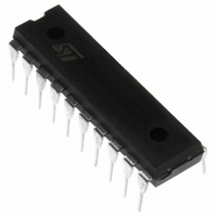
ST7FLIT19BF1B6 STMicroelectronics, ST7FLIT19BF1B6 Datasheet - Page 68

ST7FLIT19BF1B6
Manufacturer Part Number
ST7FLIT19BF1B6
Description
IC MCU 8BIT 4K FLASH 20DIP
Manufacturer
STMicroelectronics
Series
ST7r
Datasheet
1.ST7FLIT15BY1M6.pdf
(159 pages)
Specifications of ST7FLIT19BF1B6
Core Processor
ST7
Core Size
8-Bit
Speed
8MHz
Connectivity
SPI
Peripherals
LVD, POR, PWM, WDT
Number Of I /o
17
Program Memory Size
4KB (4K x 8)
Program Memory Type
FLASH
Eeprom Size
128 x 8
Ram Size
256 x 8
Voltage - Supply (vcc/vdd)
2.7 V ~ 5.5 V
Data Converters
A/D 7x10b
Oscillator Type
Internal
Operating Temperature
-40°C ~ 85°C
Package / Case
20-DIP (0.300", 7.62mm)
Processor Series
ST7FLIT1x
Core
ST7
Data Bus Width
8 bit
Data Ram Size
256 B
Interface Type
SPI
Maximum Clock Frequency
8 MHz
Number Of Programmable I/os
17
Number Of Timers
4
Operating Supply Voltage
2.7 V to 5.5 V
Maximum Operating Temperature
+ 85 C
Mounting Style
Through Hole
Development Tools By Supplier
ST7FLITE-SK/RAIS, ST7FLIT1B-D/RAIS, ST7MDT10-DVP3, ST7MDT10-EMU3, STX-RLINK
Minimum Operating Temperature
- 40 C
On-chip Adc
10 bit , 13 bit, 7 Channel
For Use With
497-6232 - BOARD EVAL ST7LITE1B,STP5NK60Z497-5049 - KIT STARTER RAISONANCE ST7FLITE497-5046 - KIT TOOL FOR ST7/UPSD/STR7 MCU
Lead Free Status / RoHS Status
Lead free / RoHS Compliant
Other names
497-5626-5
Available stocks
Company
Part Number
Manufacturer
Quantity
Price
Company:
Part Number:
ST7FLIT19BF1B6
Manufacturer:
TE
Quantity:
1 000
ST7LITE1xB
DUAL 12-BIT AUTORELOAD TIMER 4 (Cont’d)
8. Set the OP_EN bit in the PWM3CSR register to
enable one-pulse mode.
9. Enable the PWM3 output by setting the OE3 bit
in the PWMCR register.
The "Wait for Overflow event" in step 6 can be re-
placed by forced update (writing the FORCE2 bit).
Figure 47. Block Diagram of One Pulse Mode
Figure 48. One Pulse Mode and PWM Timing Diagram
68/159
1
LTIC pin
Note 1: When OP_EN=0, LTIC edges are not taken into account as the timer runs in PWM mode.
PWM3CSR Register
f
f
counter2
counter2
CNTR2
LTIC
CNTR2
LTIC
PWM2/3
PWM2/3
Edge
Selection
OPEDGE
OVF
ATR2
000
OP_EN
DCR2/3
DCR2/3
12-bit AutoReload Register 2
12-bit Active DCR2/3
OVF
Follow the same procedure for PWM2 with the bits
corresponding to PWM2.
Note: When break is applied in one-pulse mode,
the CNTR2, DCR2/3 & ATR2 registers are reset.
Consequently, these registers have to be initial-
ized again when break is removed.
12-bit Upcounter 2
ATR2
000
OP2/3
DCR2/3
DCR2/3
Generation
PWM
OVF
ATR2
ATR2
PWM2/3
000


