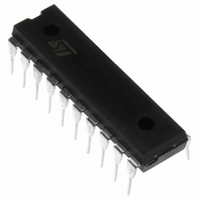
ST7FLIT19BF1B6 STMicroelectronics, ST7FLIT19BF1B6 Datasheet - Page 73

ST7FLIT19BF1B6
Manufacturer Part Number
ST7FLIT19BF1B6
Description
IC MCU 8BIT 4K FLASH 20DIP
Manufacturer
STMicroelectronics
Series
ST7r
Datasheet
1.ST7FLIT15BY1M6.pdf
(159 pages)
Specifications of ST7FLIT19BF1B6
Core Processor
ST7
Core Size
8-Bit
Speed
8MHz
Connectivity
SPI
Peripherals
LVD, POR, PWM, WDT
Number Of I /o
17
Program Memory Size
4KB (4K x 8)
Program Memory Type
FLASH
Eeprom Size
128 x 8
Ram Size
256 x 8
Voltage - Supply (vcc/vdd)
2.7 V ~ 5.5 V
Data Converters
A/D 7x10b
Oscillator Type
Internal
Operating Temperature
-40°C ~ 85°C
Package / Case
20-DIP (0.300", 7.62mm)
Processor Series
ST7FLIT1x
Core
ST7
Data Bus Width
8 bit
Data Ram Size
256 B
Interface Type
SPI
Maximum Clock Frequency
8 MHz
Number Of Programmable I/os
17
Number Of Timers
4
Operating Supply Voltage
2.7 V to 5.5 V
Maximum Operating Temperature
+ 85 C
Mounting Style
Through Hole
Development Tools By Supplier
ST7FLITE-SK/RAIS, ST7FLIT1B-D/RAIS, ST7MDT10-DVP3, ST7MDT10-EMU3, STX-RLINK
Minimum Operating Temperature
- 40 C
On-chip Adc
10 bit , 13 bit, 7 Channel
For Use With
497-6232 - BOARD EVAL ST7LITE1B,STP5NK60Z497-5049 - KIT STARTER RAISONANCE ST7FLITE497-5046 - KIT TOOL FOR ST7/UPSD/STR7 MCU
Lead Free Status / RoHS Status
Lead free / RoHS Compliant
Other names
497-5626-5
Available stocks
Company
Part Number
Manufacturer
Quantity
Price
Company:
Part Number:
ST7FLIT19BF1B6
Manufacturer:
TE
Quantity:
1 000
DUAL 12-BIT AUTORELOAD TIMER 4 (Cont’d)
AUTORELOAD REGISTER (ATR1H)
Read / Write
Reset Value: 0000 0000 (00h)
AUTORELOAD REGISTER (ATR1L)
Read / Write
Reset Value: 0000 0000 (00h)
Bits 11:0 = ATR1[11:0] Autoreload Register 1.
This is a 12-bit register which is written by soft-
ware. The ATR1 register value is automatically
loaded into the upcounter CNTR1 when an over-
flow occurs. The register value is used to set the
PWM frequency.
PWM OUTPUT CONTROL REGISTER
(PWMCR)
Read/Write
Reset Value: 0000 0000 (00h)
Bits 7:0 = OE[3:0] PWMx output enable.
These bits are set and cleared by software and
cleared by hardware after a reset.
0: PWM mode disabled. PWMx Output Alternate
1: PWM mode enabled
ATR7
15
Function disabled (I/O pin free for general pur-
pose I/O)
0
7
7
0
ATR6
OE3
0
ATR5
0
0
ATR4
OE2
0
ATR11 ATR10 ATR9
ATR3
0
ATR2
OE1
ATR1
0
ATR0
ATR8
OE0
0
0
8
PWMx CONTROL STATUS REGISTER
(PWMxCSR)
Read / Write
Reset Value: 0000 0000 (00h)
Bits 7:4= Reserved, must be kept cleared.
Bit 3 = OP_EN One Pulse Mode Enable
This bit is read/write by software and cleared by
hardware after a reset. This bit enables the One
Pulse feature for PWM2 and PWM3. (Only availa-
ble for PWM3CSR)
0: One Pulse mode disabled for PWM2/3.
1: One Pulse mode enabled for PWM2/3.
Bit 2 = OPEDGE One Pulse Edge Selection.
This bit is read/write by software and cleared by
hardware after a reset. This bit selects the polarity
of the LTIC signal for One Pulse feature. This bit
will be effective only if OP_EN bit is set. (Only
available for PWM3CSR)
0: Falling edge of LTIC is selected.
1: Rising edge of LTIC is selected.
Bit 1 = OPx PWMx Output Polarity.
This bit is read/write by software and cleared by
hardware after a reset. This bit selects the polarity
of the PWM signal.
0: The PWM signal is not inverted.
1: The PWM signal is inverted.
Bit 0 = CMPFx PWMx Compare Flag.
This bit is set by hardware and cleared by software
by reading the PWMxCSR register. It indicates
that the upcounter value matches the Active DCRx
register value.
0: Upcounter value does not match DCRx value.
1: Upcounter value matches DCRx value.
7
0
0
0
0
OP_EN
OPEDG
E
ST7LITE1xB
OPx CMPFx
73/159
0
1


