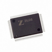
Z16F3211FI20SG Zilog, Z16F3211FI20SG Datasheet - Page 231

Z16F3211FI20SG
Manufacturer Part Number
Z16F3211FI20SG
Description
IC ZNEO MCU FLASH 32K 80QFP
Manufacturer
Zilog
Series
Encore!® ZNEOr
Datasheet
1.Z16F2800100ZCOG.pdf
(388 pages)
Specifications of Z16F3211FI20SG
Core Processor
ZNEO
Core Size
16-Bit
Speed
20MHz
Connectivity
EBI/EMI, I²C, IrDA, LIN, SPI, UART/USART
Peripherals
Brown-out Detect/Reset, DMA, POR, PWM, WDT
Number Of I /o
60
Program Memory Size
32KB (32K x 8)
Program Memory Type
FLASH
Ram Size
2K x 8
Voltage - Supply (vcc/vdd)
2.7 V ~ 3.6 V
Data Converters
A/D 12x10b
Oscillator Type
Internal
Operating Temperature
0°C ~ 70°C
Package / Case
80-BQFP
Processor Series
Z16F3x
Core
Zneo
Data Bus Width
16 bit
Data Ram Size
2 B
Interface Type
ESPI, I2C, UART
Maximum Clock Frequency
20 MHz
Number Of Programmable I/os
60
Number Of Timers
4
Operating Supply Voltage
2.7 V to 3.6 V
Maximum Operating Temperature
+ 70 C
Mounting Style
SMD/SMT
Development Tools By Supplier
Z16F2800100ZCOG
Minimum Operating Temperature
0 C
On-chip Adc
10 bit, 12 Channel
For Use With
770-1003 - ISP 4PORT FOR ZILOG ZNEO MCU269-4537 - DEV KIT FOR Z16F ZNEO
Lead Free Status / RoHS Status
Lead free / RoHS Compliant
Eeprom Size
-
Lead Free Status / Rohs Status
Details
Other names
269-4569
Available stocks
Company
Part Number
Manufacturer
Quantity
Price
Company:
Part Number:
Z16F3211FI20SG
Manufacturer:
Zilog
Quantity:
131
- Current page: 231 of 388
- Download datasheet (22Mb)
PS022008-0810
S
Slave Address
1st Byte
Figure 46. Data Transfer Format - Master Read Transaction with 10-Bit Address
12. If there are more bytes to transfer, the I
13. A NAK interrupt (
14. Software responds by setting the STOP bit of the I
15. A STOP condition is sent to the I
Master Read Transaction with a 10-Bit Address
Figure 46
The first seven bits transmitted in the first byte are
most-significant bits of the 10-bit address. The lowest bit of the first byte transferred is the
write control bit.
The data transfer procedure for a read operation to a 10-bit addressed Slave is as follows:
1. Software initializes the MODE field in the I
2. Software writes
3. Software asserts the
4. The I
5. The I
6. When the first bit is shifted out, a Transmit interrupt asserts.
7. Software responds by writing the least significant eight bits of address to the I
8. The I
9. The I
with 7-bit or 10-bit addressing (I
The MODE field selects the address width for this node when addressed as a Slave,
not for the remote Slave. Software asserts the IEN bit in the I
(write) to the I
register.
register.
High period of SCL.
If the slave does not acknowledge the address byte, the I
bit in the I
register. Software responds to the Not Acknowledge interrupt by setting the STOP bit
and clearing the TXI bit. The I
W=0 A Slave Address
2
2
2
2
displays the read transaction format for a 10-bit addressed Slave.
C Controller sends the Start condition.
C Controller loads the I
C Controller completes shifting of the first address byte.
C Slave sends an acknowledge by pulling the SDA signal Low during the next
2
C Status register, sets the
2nd Byte
2
C Data register.
11110B
NCKI
START
P R E L I M I N A R Y
bit in I2CISTAT) is generated by the I
followed by the two most significant address bits and a 0
A S Slave Address
bit of the I
2
2
C Shift register with the contents of the I
C Controller flushes the transmit data register, sends
2
2
C bus protocol allows mixing Slave address types).
C Slave.
1st Byte
ACKV
2
2
C Control register.
C Controller returns to step 7.
bit and clears the
2
C Mode register for Master/Slave mode
11110XX
2
R=1
C Control register.
2
. The two bits
A
C Controller sets the NCKI
I
2
C Master/Slave Controller
Product Specification
ACK
Data
2
2
C Control register.
ZNEO
C Controller.
bit in the I
A
XX
Z16F Series
2
Data
C Data
are the two
2
C State
2
C Data
A P
215
Related parts for Z16F3211FI20SG
Image
Part Number
Description
Manufacturer
Datasheet
Request
R

Part Number:
Description:
Communication Controllers, ZILOG INTELLIGENT PERIPHERAL CONTROLLER (ZIP)
Manufacturer:
Zilog, Inc.
Datasheet:

Part Number:
Description:
KIT DEV FOR Z8 ENCORE 16K TO 64K
Manufacturer:
Zilog
Datasheet:

Part Number:
Description:
KIT DEV Z8 ENCORE XP 28-PIN
Manufacturer:
Zilog
Datasheet:

Part Number:
Description:
DEV KIT FOR Z8 ENCORE 8K/4K
Manufacturer:
Zilog
Datasheet:

Part Number:
Description:
KIT DEV Z8 ENCORE XP 28-PIN
Manufacturer:
Zilog
Datasheet:

Part Number:
Description:
DEV KIT FOR Z8 ENCORE 4K TO 8K
Manufacturer:
Zilog
Datasheet:

Part Number:
Description:
CMOS Z8 microcontroller. ROM 16 Kbytes, RAM 256 bytes, speed 16 MHz, 32 lines I/O, 3.0V to 5.5V
Manufacturer:
Zilog, Inc.
Datasheet:

Part Number:
Description:
Low-cost microcontroller. 512 bytes ROM, 61 bytes RAM, 8 MHz
Manufacturer:
Zilog, Inc.
Datasheet:

Part Number:
Description:
Z8 4K OTP Microcontroller
Manufacturer:
Zilog, Inc.
Datasheet:

Part Number:
Description:
CMOS SUPER8 ROMLESS MCU
Manufacturer:
Zilog, Inc.
Datasheet:

Part Number:
Description:
SL1866 CMOSZ8 OTP Microcontroller
Manufacturer:
Zilog, Inc.
Datasheet:

Part Number:
Description:
SL1866 CMOSZ8 OTP Microcontroller
Manufacturer:
Zilog, Inc.
Datasheet:

Part Number:
Description:
OTP (KB) = 1, RAM = 125, Speed = 12, I/O = 14, 8-bit Timers = 2, Comm Interfaces Other Features = Por, LV Protect, Voltage = 4.5-5.5V
Manufacturer:
Zilog, Inc.
Datasheet:

Part Number:
Description:
Manufacturer:
Zilog, Inc.
Datasheet:


