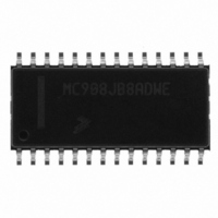
MC908JB8ADWE Freescale Semiconductor, MC908JB8ADWE Datasheet - Page 210

MC908JB8ADWE
Manufacturer Part Number
MC908JB8ADWE
Description
IC MCU 3MHZ 8K FLASH 28-SOIC
Manufacturer
Freescale Semiconductor
Series
HC08r
Datasheet
1.MC908JB8JDWE.pdf
(286 pages)
Specifications of MC908JB8ADWE
Core Processor
HC08
Core Size
8-Bit
Speed
3MHz
Connectivity
USB
Peripherals
LVD, POR, PWM
Number Of I /o
21
Program Memory Size
8KB (8K x 8)
Program Memory Type
FLASH
Ram Size
256 x 8
Voltage - Supply (vcc/vdd)
4 V ~ 5.5 V
Oscillator Type
Internal
Operating Temperature
0°C ~ 70°C
Package / Case
28-SOIC (7.5mm Width)
Processor Series
HC08JB
Core
HC08
Data Bus Width
8 bit
Data Ram Size
256 B
Interface Type
USB
Maximum Clock Frequency
3 MHz
Number Of Programmable I/os
37
Number Of Timers
2
Operating Supply Voltage
5.25 V
Maximum Operating Temperature
+ 70 C
Mounting Style
SMD/SMT
Development Tools By Supplier
FSICEBASE, DEMO908GZ60E, M68EML08GZE, KITUSBSPIDGLEVME, KITUSBSPIEVME, KIT33810EKEVME
Minimum Operating Temperature
0 C
Controller Family/series
HC08
No. Of I/o's
21
Ram Memory Size
256Byte
Cpu Speed
8MHz
No. Of Timers
1
Embedded Interface Type
SCI, SPI
Rohs Compliant
Yes
Lead Free Status / RoHS Status
Lead free / RoHS Compliant
Eeprom Size
-
Data Converters
-
Lead Free Status / Rohs Status
Lead free / RoHS Compliant
Available stocks
Company
Part Number
Manufacturer
Quantity
Price
Part Number:
MC908JB8ADWE
Manufacturer:
FREESCALE
Quantity:
20 000
- Current page: 210 of 286
- Download datasheet (2Mb)
Input/Output Ports (I/O)
12.6.1 Port D Data Register
Technical Data
210
NOTE:
NOTE:
Additional
Function:
Address:
The port D data register contains a data latch for each of the eight port D
pins.
PTD7–PTD2 are not available in the 20-pin PDIP and 20-pin SOIC
packages. PTD7 is not available in the 28-pin SOIC package.
PTD[7:0] — Port D Data Bits
In 20-pin package, PTD1 and PTD0 are bonded together to PTD0/1 pin,
forming a 50mA high current sink pin. When both PTD1 and PTD0 are
configured as output, the values of PTD0 and PTD1 should be written
the same.
Reset:
Read:
Write:
These read/write bits are software programmable. Data direction of
each port D pin is under control of the corresponding bit in data
direction register D. Reset has no effect on port D data.
The LED direct drive bit, PTDLDD, in the port option control register
(POCR) controls the drive options for the PTD5–PTD2 pins. The
infrared LED drive bit, PTDILDD, in the POCR controls the drive
options for the PTD1–PTD0 pins. (See
Open-drain Open-drain Open-drain Open-drain Open-drain Open-drain Open-drain Open-drain
$0003
PTD7
Bit 7
Figure 12-11. Port D Data Register (PTD)
Input/Output Ports (I/O)
PTD6
6
MC68HC908JB8•MC68HC08JB8•MC68HC08JT8 — Rev. 2.3
10mA
PTD5
sink
5
Unaffected by reset
10mA
PTD4
sink
4
10mA
PTD3
sink
12.8 Port
3
10mA
PTD2
sink
Freescale Semiconductor
2
Options.)
25mA
PTD1
sink
1
25mA
PTD0
Bit 0
sink
Related parts for MC908JB8ADWE
Image
Part Number
Description
Manufacturer
Datasheet
Request
R
Part Number:
Description:
Manufacturer:
Freescale Semiconductor, Inc
Datasheet:
Part Number:
Description:
Manufacturer:
Freescale Semiconductor, Inc
Datasheet:
Part Number:
Description:
Manufacturer:
Freescale Semiconductor, Inc
Datasheet:
Part Number:
Description:
Manufacturer:
Freescale Semiconductor, Inc
Datasheet:
Part Number:
Description:
Manufacturer:
Freescale Semiconductor, Inc
Datasheet:
Part Number:
Description:
Manufacturer:
Freescale Semiconductor, Inc
Datasheet:
Part Number:
Description:
Manufacturer:
Freescale Semiconductor, Inc
Datasheet:
Part Number:
Description:
Manufacturer:
Freescale Semiconductor, Inc
Datasheet:
Part Number:
Description:
Manufacturer:
Freescale Semiconductor, Inc
Datasheet:
Part Number:
Description:
Manufacturer:
Freescale Semiconductor, Inc
Datasheet:
Part Number:
Description:
Manufacturer:
Freescale Semiconductor, Inc
Datasheet:
Part Number:
Description:
Manufacturer:
Freescale Semiconductor, Inc
Datasheet:
Part Number:
Description:
Manufacturer:
Freescale Semiconductor, Inc
Datasheet:
Part Number:
Description:
Manufacturer:
Freescale Semiconductor, Inc
Datasheet:
Part Number:
Description:
Manufacturer:
Freescale Semiconductor, Inc
Datasheet:


