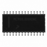
MC908JB8ADWE Freescale Semiconductor, MC908JB8ADWE Datasheet - Page 214

MC908JB8ADWE
Manufacturer Part Number
MC908JB8ADWE
Description
IC MCU 3MHZ 8K FLASH 28-SOIC
Manufacturer
Freescale Semiconductor
Series
HC08r
Datasheet
1.MC908JB8JDWE.pdf
(286 pages)
Specifications of MC908JB8ADWE
Core Processor
HC08
Core Size
8-Bit
Speed
3MHz
Connectivity
USB
Peripherals
LVD, POR, PWM
Number Of I /o
21
Program Memory Size
8KB (8K x 8)
Program Memory Type
FLASH
Ram Size
256 x 8
Voltage - Supply (vcc/vdd)
4 V ~ 5.5 V
Oscillator Type
Internal
Operating Temperature
0°C ~ 70°C
Package / Case
28-SOIC (7.5mm Width)
Processor Series
HC08JB
Core
HC08
Data Bus Width
8 bit
Data Ram Size
256 B
Interface Type
USB
Maximum Clock Frequency
3 MHz
Number Of Programmable I/os
37
Number Of Timers
2
Operating Supply Voltage
5.25 V
Maximum Operating Temperature
+ 70 C
Mounting Style
SMD/SMT
Development Tools By Supplier
FSICEBASE, DEMO908GZ60E, M68EML08GZE, KITUSBSPIDGLEVME, KITUSBSPIEVME, KIT33810EKEVME
Minimum Operating Temperature
0 C
Controller Family/series
HC08
No. Of I/o's
21
Ram Memory Size
256Byte
Cpu Speed
8MHz
No. Of Timers
1
Embedded Interface Type
SCI, SPI
Rohs Compliant
Yes
Lead Free Status / RoHS Status
Lead free / RoHS Compliant
Eeprom Size
-
Data Converters
-
Lead Free Status / Rohs Status
Lead free / RoHS Compliant
Available stocks
Company
Part Number
Manufacturer
Quantity
Price
Part Number:
MC908JB8ADWE
Manufacturer:
FREESCALE
Quantity:
20 000
- Current page: 214 of 286
- Download datasheet (2Mb)
Input/Output Ports (I/O)
Technical Data
214
NOTE:
NOTE:
D– and D+ — USB Data Pins
PTE4/D– pin has two programmable pullup resistors. One is used for
PTE4 when the USB module is disabled and another is used for D–
when the USB module is enabled.
TCH1–TCH0 — Timer Channel I/O Bits
TCLK — Timer Clock Input
Data direction register E (DDRE) does not affect the data direction of
port E pins that are being used by the TIM. However, the DDRE bits
always determine whether reading port E returns the states of the
latches or the states of the pins.
PTE4 pin functions as an external interrupt when PTE4IE=1 in the
IRQ option control register (IOCR) and USBEN=0 in the USB address
register (USB disabled). (See
D– and D+ are the differential data lines used by the USB module.
(See
The USB module enable bit, USBEN, in the USB address register
(UADDR) controls the pin options for PTE4/D– and PTE3/D+. When
the USB module is enabled, PTE4/D– and PTE3/D+ function as USB
data pins D– and D+. When the USB module is disabled, PTE4/D–
and PTE3/D+ function as 10mA open-drain pins for PS/2 clock and
data use.
The Pullup enable bit, PULLEN, in the USB control register 3 (UCR3)
enables a 1.5kΩ pullup on D– pin when the USB module is enabled.
(See
The PTE2/TCH1–PTE1/TCH0 pins are the TIM input capture/output
compare pins. The edge/level select bits, ELSxB and ELSxA,
determine whether the PTE2/TCH1–PTE1/TCH0 pins are timer
channel I/O pins or general-purpose I/O pins. (See
Interface Module
The PTE0/TCLK pin is the external clock input for the TIM. The
prescaler select bits, PS[2:0], select PTE0/TCLK as the TIM clock
input. When not selected as the TIM clock, PTE0/TCLK is available
for general purpose I/O. (See
(TIM).)
Section 9. Universal Serial Bus Module
9.8.8 USB Control Register
Input/Output Ports (I/O)
MC68HC908JB8•MC68HC08JB8•MC68HC08JT8 — Rev. 2.3
(TIM).)
Section 11. Timer Interface Module
13.9 IRQ Option Control
3.)
Freescale Semiconductor
(USB).)
Section 11. Timer
Register.)
Related parts for MC908JB8ADWE
Image
Part Number
Description
Manufacturer
Datasheet
Request
R
Part Number:
Description:
Manufacturer:
Freescale Semiconductor, Inc
Datasheet:
Part Number:
Description:
Manufacturer:
Freescale Semiconductor, Inc
Datasheet:
Part Number:
Description:
Manufacturer:
Freescale Semiconductor, Inc
Datasheet:
Part Number:
Description:
Manufacturer:
Freescale Semiconductor, Inc
Datasheet:
Part Number:
Description:
Manufacturer:
Freescale Semiconductor, Inc
Datasheet:
Part Number:
Description:
Manufacturer:
Freescale Semiconductor, Inc
Datasheet:
Part Number:
Description:
Manufacturer:
Freescale Semiconductor, Inc
Datasheet:
Part Number:
Description:
Manufacturer:
Freescale Semiconductor, Inc
Datasheet:
Part Number:
Description:
Manufacturer:
Freescale Semiconductor, Inc
Datasheet:
Part Number:
Description:
Manufacturer:
Freescale Semiconductor, Inc
Datasheet:
Part Number:
Description:
Manufacturer:
Freescale Semiconductor, Inc
Datasheet:
Part Number:
Description:
Manufacturer:
Freescale Semiconductor, Inc
Datasheet:
Part Number:
Description:
Manufacturer:
Freescale Semiconductor, Inc
Datasheet:
Part Number:
Description:
Manufacturer:
Freescale Semiconductor, Inc
Datasheet:
Part Number:
Description:
Manufacturer:
Freescale Semiconductor, Inc
Datasheet:


