MC9S08DZ60ACLF Freescale Semiconductor, MC9S08DZ60ACLF Datasheet
MC9S08DZ60ACLF
Specifications of MC9S08DZ60ACLF
Available stocks


Related parts for MC9S08DZ60ACLF

MC9S08DZ60ACLF Summary of contents
Page 1
MC9S08DZ128 MC9S08DZ96 MC9S08DV128 MC9S08DV96 Data Sheet HCS08 Microcontrollers MC9S08DZ128 Rev. 1 5/2008 freescale.com ...
Page 2
...
Page 3
MC9S08DZ128 Series Features 8-Bit HCS08 Central Processor Unit (CPU) • 40-MHz HCS08 CPU (20-MHz bus) • HC08 instruction set with added BGND instruction • Support for interrupt/reset sources On-Chip Memory • FLASH read/program/erase over full operating voltage ...
Page 4
...
Page 5
... MC9S08DZ128 Series Data Sheet Freescale™ and the Freescale logo are trademarks of Freescale Semiconductor, Inc. © Freescale Semiconductor, Inc., 2007, 2008. All rights reserved. Covers: MC9S08DZ128 MC9S08DZ96 MC9S08DV128 MC9S08DV96 MC9S08DZ128 Rev. 1 5/2008 ...
Page 6
... The following revision history table summarizes changes contained in this document. Revision Revision Number Date 1 4/2008 Initial Release © Freescale Semiconductor, Inc., 2007, 2008. All rights reserved. This product incorporates SuperFlash 6 Description of Changes ® Technology licensed from SST. MC9S08DZ128 Series Data Sheet, Rev. 1 Freescale Semiconductor ...
Page 7
... Real-Time Counter (S08RTCV1) ................................................... 343 Chapter 16 Timer Pulse-Width Modulator (S08TPMV3) ................................. 353 Chapter 17 Development Support ................................................................... 379 Chapter 18 Debug Module (S08DBGV3) (128K).............................................. 393 Appendix A Electrical Characteristics.............................................................. 419 Appendix B Ordering Information and Mechanical Drawings........................ 447 Freescale Semiconductor List of Chapters Title MC9S08DZ128 Series Data Sheet, Rev. 1 Page 7 ...
Page 8
...
Page 9
... On-Chip Peripheral Modules in Stop Modes ....................................................................42 4.1 MC9S08DZ128 Series Memory Map ..............................................................................................45 4.2 Reset and Interrupt Vector Assignments ..........................................................................................49 4.3 Register Addresses and Bit Assignments.........................................................................................51 4.4 Memory Management Unit ..............................................................................................................61 4.4.1 Features .............................................................................................................................61 4.4.2 Memory Expansion ...........................................................................................................61 Freescale Semiconductor Contents Title Chapter 1 Device Overview Chapter 2 Pins and Connections , V ) Pins ..............................................................................33 REFH REFL ...
Page 10
... System Options Register 2 (SOPT2) ................................................................................97 5.8.6 System Device Identification Register (SDIDH, SDIDL) ................................................98 5.8.7 System Power Management Status and Control 1 Register (SPMSC1) ...........................99 5.8.8 System Power Management Status and Control 2 Register (SPMSC2) .........................100 10 Title Chapter 5 MC9S08DZ128 Series Data Sheet, Rev. 1 Page Freescale Semiconductor ...
Page 11
... Immediate Addressing Mode (IMM) ..............................................................................147 7.3.4 Direct Addressing Mode (DIR) ......................................................................................148 7.3.5 Extended Addressing Mode (EXT) ................................................................................148 7.3.6 Indexed Addressing Mode ..............................................................................................148 7.4 Special Operations..........................................................................................................................149 7.4.1 Reset Sequence ...............................................................................................................149 Freescale Semiconductor Title Chapter 6 Parallel Input/Output Control Chapter 7 MC9S08DZ128 Series Data Sheet, Rev. 1 Page ...
Page 12
... Calibrating the Internal Reference Clock (IRC) .............................................................195 5-V Analog Comparator (S08ACMPV3) 9.1 Introduction ....................................................................................................................................199 9.1.1 ACMP Configuration Information ..................................................................................199 9.1.2 Features ...........................................................................................................................201 9.1.3 Modes of Operation ........................................................................................................201 9.1.4 Block Diagram ................................................................................................................201 9.2 External Signal Description ...........................................................................................................203 12 Title Chapter 8 Chapter 9 MC9S08DZ128 Series Data Sheet, Rev. 1 Page Freescale Semiconductor ...
Page 13
... Automatic Compare Function .........................................................................................225 10.4.6 MCU Wait Mode Operation ............................................................................................225 10.4.7 MCU Stop3 Mode Operation ..........................................................................................226 10.4.8 MCU Stop2 Mode Operation ..........................................................................................226 10.5 Initialization Information ...............................................................................................................227 10.5.1 ADC Module Initialization Example .............................................................................227 Freescale Semiconductor Title Chapter 10 ) ..................................................................................................213 DDAD ) .................................................................................................213 SSAD ) ...
Page 14
... Modes of Operation ........................................................................................................255 12.1.3 Block Diagram ................................................................................................................256 12.2 External Signal Description ...........................................................................................................256 12.2.1 RXCAN — CAN Receiver Input Pin .............................................................................256 12.2.2 TXCAN — CAN Transmitter Output Pin .....................................................................256 12.2.3 CAN System ...................................................................................................................256 14 Title Chapter 11 Chapter 12 MC9S08DZ128 Series Data Sheet, Rev. 1 Page Freescale Semiconductor ...
Page 15
... Initialization/Application Information ...........................................................................................304 12.6.1 MSCAN initialization .....................................................................................................304 12.6.2 Bus-Off Recovery ...........................................................................................................305 Serial Peripheral Interface (S08SPIV3) 13.1 Introduction ....................................................................................................................................307 13.1.1 Features ...........................................................................................................................309 13.1.2 Block Diagrams ..............................................................................................................309 13.1.3 SPI Baud Rate Generation ..............................................................................................311 Freescale Semiconductor Title Chapter 13 MC9S08DZ128 Series Data Sheet, Rev. 1 Page 15 ...
Page 16
... SCI Data Register (SCIxD) .............................................................................................335 14.3 Functional Description ...................................................................................................................335 14.3.1 Baud Rate Generation .....................................................................................................335 14.3.2 Transmitter Functional Description ................................................................................336 14.3.3 Receiver Functional Description .....................................................................................337 14.3.4 Interrupts and Status Flags ..............................................................................................339 14.3.5 Additional SCI Functions ...............................................................................................340 16 Title Chapter 14 MC9S08DZ128 Series Data Sheet, Rev. 1 Page Freescale Semiconductor ...
Page 17
... Reset Overview ..............................................................................................................................374 16.5.1 General ............................................................................................................................374 16.5.2 Description of Reset Operation .......................................................................................374 16.6 Interrupts ........................................................................................................................................374 16.6.1 General ............................................................................................................................374 16.6.2 Description of Interrupt Operation ..................................................................................375 16.7 The Differences from TPM v2 to TPM v3.....................................................................................376 Freescale Semiconductor Title Chapter 15 Chapter 16 MC9S08DZ128 Series Data Sheet, Rev. 1 Page 17 ...
Page 18
... Interrupts ........................................................................................................................................417 18.7 Electrical Specifications .................................................................................................................417 A.1 Introduction ...................................................................................................................................419 A.2 Parameter Classification ................................................................................................................419 A.3 Absolute Maximum Ratings ..........................................................................................................419 A.4 Thermal Characteristics .................................................................................................................420 18 Title Chapter 17 Development Support Chapter 18 Appendix A Electrical Characteristics MC9S08DZ128 Series Data Sheet, Rev. 1 Page 396 Freescale Semiconductor ...
Page 19
... A.13 FLASH and EEPROM ..................................................................................................................445 A.14 EMC Performance .........................................................................................................................446 A.14.1 Radiated Emissions .........................................................................................................446 Ordering Information and Mechanical Drawings B.1 Ordering Information ....................................................................................................................447 B.1.1 MC9S08DZ128 Series Devices ......................................................................................447 B.2 Mechanical Drawings ....................................................................................................................448 Freescale Semiconductor Title Appendix B MC9S08DZ128 Series Data Sheet, Rev. 1 Page 19 ...
Page 20
...
Page 21
... Devices in the MC9S08DZ128 Series This data sheet covers members of the MC9S08DZ128 Series of MCUs: • MC9S08DZ128 • MC9S08DZ96 • MC9S08DV128 • MC9S08DV96 Table 1-1 summarizes the feature set available in the MC9S08DZ128 Series. Freescale Semiconductor MC9S08DZ128 Series Data Sheet, Rev ...
Page 22
... MC9S08DV96 131,072 98,304 6016 4096 — — 100 yes yes 1 1 yes yes yes yes yes yes yes no no yes yes yes yes yes yes yes yes yes yes yes yes yes yes no no yes yes yes yes yes Freescale Semiconductor ...
Page 23
... Freescale’s Controller Area Network Serial Peripheral Interface Serial Communications Interface Real-Time Counter Timer Pulse Width Modulator 1.2 MCU Block Diagram Figure 1-1 is the MC9S08DZ128 Series system-level block diagram. Freescale Semiconductor Table 1-2. Module Versions Module (CPU) (ACMP_5V) (ADC) (DBG) (IIC) (MCG) ...
Page 24
... PTD3/PID3/TPM1CH1 PTD2/PID2/TPM1CH0 PTD1/PID1/TPM2CH1 PTD0/PID0/TPM2CH0 PTE7/RxD2/RXCAN PTE6/TxD2/TXCAN PTE5/SDA1/MISO1 PTE4/SCL1/MOSI1 PTE3/SPSCK1 PTE2/SS1 PTE1/RxD1 PTE0/TxD1 ● PTF7 ● PTF6/ACMP2O PTF5/ACMP2- PTF4/ACMP2+ PTF3/TPM2CLK/SDA1 PTF2/TPM1CLK/SCL1 PTF1/RxD2 PTF0/TxD2 PTG7/SDA2 PTG6/SCL2 ● PTG5 ● CLOCK PTG4 ● PTG3 (MCG) ● PTG2 XTAL PTG1/XTAL EXTAL (XOSC) PTG0/EXTAL Freescale Semiconductor ...
Page 25
... MCGLCLK XOSC CPU EXTAL XTAL * The fixed frequency clock (FFCLK) is internally synchronized to the bus clock and must not exceed one half of the bus clock frequency. Freescale Semiconductor TPM1CLK TPM2CLK TPM3CLK TPM1 TPM2 TPM3 COP RTC FFCLK* BDC ADC has min and max frequency requirements ...
Page 26
... Chapter 1 Device Overview 26 MC9S08DZ128 Series Data Sheet, Rev. 1 Freescale Semiconductor ...
Page 27
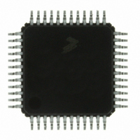
... This section describes signals that connect to package pins. It includes pinout diagrams, recommended system connections, and detailed discussions of signals. 2.1 Device Pin Assignment This section shows the pin assignments for MC9S08DZ128 Series MCUs in the available packages. Freescale Semiconductor MC9S08DZ128 Series Data Sheet, Rev ...
Page 28
... PTE1/RxD1 Figure 2-1. MC9S08DZ128 Series 28 100-Pin LQFP in 100-Pin LQFP Package MC9S08DZ128 Series Data Sheet, Rev PTB1/PIB1/ADP9 74 PTC2/ADP18 73 PTA0/PIA0/ADP0/MCLK 72 PTC1/ADP17 71 PTB0/PIB0/ADP8 70 PTC0/ADP16 PTH7 69 PTH6 68 PTH5 67 PTH4 66 65 BKGD/MS 64 PTD7/PID7/TPM1CH5 63 PTD6/PID6/TPM1CH4 PTL3 59 PTF7 58 PTH3/MISO2 57 PTH2/MOSI2 56 PTH1/SPSCK2 55 PTH0/SS2 54 PTD5/PID5/TPM1CH3 53 PTD4/PID4/TPM1CH2 52 PTD3/PID3/TPM1CH1 51 PTD2/PID2/TPM1CH0 Freescale Semiconductor ...
Page 29
... PTB6/PIB6/ADP14 PTC5/ADP21 PTA7/PIA7/ADP7/IRQ PTC6/ADP22 PTB7/PIB7/ADP15 PTC7/ADP23 PTG0/EXTAL PTG1/XTAL RESET PTF4/ACMP2+ PTF5/ACMP2- PTF6/ACMP2O PTE0/TxD1 PTE1/RxD1 Figure 2-2. MC9S08DZ128 Series Freescale Semiconductor 64-Pin 8 9 LQFP 64-Pin LQFP Package MC9S08DZ128 Series Data Sheet, Rev. 1 Chapter 2 Pins and Connections 48 PTB1/PIB1/ADP9 47 PTC2/ADP18 46 PTA0/PIA0/ADP0/MCLK 45 PTC1/ADP17 44 PTB0/PIB0/ADP8 43 PTC0/ADP16 ...
Page 30
... PTE0/TxD1 PTE1/RxD1 V Figure 2-3. MC9S08DZ128 Series 48-Pin LQFP 7 RESET and V are internally connected to V and V REFH REFL DDA in MC9S08DZ128 Series Data Sheet, Rev PTB1/PIB1/ADP9 35 PTA0/PIA0/ADP0/MCLK 34 PTB0/PIB0/ADP8 33 BKGD/MS PTD7/PID7/TPM1CH5 32 PTD6/PID6/TPM1CH4 PTD5/PID5/TPM1CH3 28 27 PTD4/PID4/TPM1CH2 PTD3/PID3/TPM1CH1 26 25 PTD2/PID2/TPM1CH0 , respectively. SSA 48-Pin LQFP Freescale Semiconductor ...
Page 31
... PTK4 PTK5 PTK6 PTK7 PTJ0/PIJ0/TPM3CH0 PTJ1/PIJ1/TPM3CH1 PTJ2/PIJ2/TPM3CH2 PTJ3/PIJ3/TPM3CH3 PTJ4/PIJ4 PTJ5/PIJ5 PTJ6/PIJ6 PTJ7/PIJ7/TPM3CLK PTH0/SS2 PTH1/SPSCK2 PTH2/MOSI2 PTH3/MISO2 PTH4 PTH5 PTH6 PTH7 Figure 2-4. Basic System Connections (Shown in 100Pin Package) Freescale Semiconductor MC9S08DZ128 0.1 μ PORT V DDA REFH 0.1 μF IRQ V REFL V SSA ...
Page 32
... MCU system. If desired, a manual external reset can be added by supplying a simple switch to ground (pull reset pin low to force a reset). 32 (when used) and R S MC9S08DZ128 Series Data Sheet, Rev. 1 pins. Each pin DD Chapter 8, “Multi-Purpose Clock should be low-inductance F Freescale Semiconductor ...
Page 33
... For information about controlling these pins as general-purpose I/O pins, see Chapter 6, “Parallel Input/Output Freescale Semiconductor , V ) Pins REFH REFL Control.” ...
Page 34
... XTAL 8 — PTL5 9 PTF4 10 PTF5 — PTF6 — PTJ4 PIJ4 — PTJ5 PIJ5 — PTJ6 PIJ6 — PTJ7 PIJ7 TPM3CLK 11 PTE0 1 12 PTE1 MC9S08DZ128 Series Data Sheet, Rev. 1 --> Highest Alt 1 Alt 2 IRQ RESET ACMP2+ ACMP2- ACMP2O TxD1 RxD1 Freescale Semiconductor ...
Page 35
... Freescale Semiconductor <-- Lowest Priority Port 48 Pin/Interrupt 13 PTE2 14 PTE3 15 PTE4 SCL1 16 PTE5 SDA1 — PTG2 — PTG3 — PTL6 — PTL7 17 PTF0 18 PTF1 19 PTF2 TPM1CLK 20 PTF3 TPM2CLK — — — PTG4 — ...
Page 36
... PTA3 PIA3 ADP3 — PTL4 — PTK0 — PTK1 — PTK2 — PTK3 42 MC9S08DZ128 Series Data Sheet, Rev. 1 --> Highest Alt 1 Alt 2 TPM1CH0 TPM1CH1 TPM1CH2 TPM1CH3 SS2 SPSCK2 MOSI2 MISO2 TPM1CH4 TPM1CH5 MS MCLK 4 4 ACMP1 ACMP1- ACMP1O V SSA V REFL Freescale Semiconductor ...
Page 37
... The default reset locations are on PTF2 and PTF3. 3 The SCI2 module pins can be repositioned using SCI2PS bit in the SOPT1 register. The default reset locations are on PTF0 and PTF1 both these analog modules are enabled they both will have access to the pin. Freescale Semiconductor <-- Lowest Priority Port 48 Pin/Interrupt 43 — ...
Page 38
... Chapter 2 Pins and Connections 38 MC9S08DZ128 Series Data Sheet, Rev. 1 Freescale Semiconductor ...
Page 39
... When encountering a BDC breakpoint • When encountering a DBG breakpoint After entering active background mode, the CPU is held in a suspended state waiting for serial background commands rather than executing instructions from the user application program. Freescale Semiconductor MC9S08DZ128 Series Data Sheet, Rev ...
Page 40
... MCU is operated in run mode for the first time. When the MC9S08DZ128 Series is shipped from the Freescale Semiconductor factory, the FLASH program memory is erased by default unless specifically noted so there is no program that could be executed in run mode until the FLASH memory is initially programmed ...
Page 41
... CPU executes a STOP instruction, then the voltage regulator remains active during stop mode. For the ADC to operate or for the ACMP to be used when comparing with an internal voltage, the LVD must be left enabled when entering stop3. Freescale Semiconductor Chapter 8, “Multi-Purpose Clock Generator Table 3-1. Stop Mode Selection ...
Page 42
... When the MCU enters any stop mode, system clocks to the internal peripheral modules are stopped. Even in the exception case (ENBDM = 1), where clocks to the background debug logic continue to operate, 42 Support.” If ENBDM is set when the CPU executes a MC9S08DZ128 Series Data Sheet, Rev. 1 Table 3-1. Most is below the LVD DD Freescale Semiconductor ...
Page 43
... Requires the LVD or BDC to be enabled. 6 ERCLKEN and EREFSTEN set in MCGC2 for, else in standby. For high frequency range (RANGE in MCGC2 set) requires the LVD to also be enabled in stop3. Freescale Semiconductor Mode” for specific information on system behavior in stop modes. Table 3-2. Stop Mode Behavior Mode ...
Page 44
... Chapter 3 Modes of Operation 44 MC9S08DZ128 Series Data Sheet, Rev. 1 Freescale Semiconductor ...
Page 45
... I/O and control/status registers. The registers are divided into three groups: • Direct-page registers (0x0000 through 0x007F) • High-page registers (0x1800 through 0x18FF) • Nonvolatile registers (0xFFB0 through 0xFFBF) Freescale Semiconductor MC9S08DZ128 Series Data Sheet, Rev ...
Page 46
... MC9S08DZ128 Series Data Sheet, Rev. 1 also be accessed through the linear address pointer. Extended Address 0x1_C000 - 0x1_FFFF 0x1_8000 - 0x1_BFFF 0x1_4000 - 0x1_7FFF 0x1_0000 - 0x1_3FFF 0x0_C000 - 0x0_FFFF 0x0_8000 - 0x0_BFFF 0x0_4000 - 0x0_7FFF FLASH 16384 BYTES Section 4.6.10, “EEPROM Mapping” for more Freescale Semiconductor ...
Page 47
... PPAGE and CPU addresses 0x0_BFFF 0x0_C000 PPAGE=3 16384 BYTES 0x0_FFFF 1 EEPROM address range shows half the total EEPROM. See Freescale Semiconductor CPU Address 0x0000 All 96K bytes of Flash can 0x007F also be accessed through 0x0080 the linear address pointer. RAM ...
Page 48
... FLASH 0x7FFF 0x8000 0x0_0000 - 0x0_3FFF A13:A0 0xBFFF 0xC000 FLASH 0xFFFF Figure 4-3. MC9S08DV128 Memory Map MC9S08DZ128 Series Data Sheet, Rev. 1 Extended Address 0x1_C000 - 0x1_FFFF 0x1_8000 - 0x1_BFFF 0x1_4000 - 0x1_7FFF 0x1_0000 - 0x1_3FFF 0x0_C000 - 0x0_FFFF 0x0_8000 - 0x0_BFFF 0x0_4000 - 0x0_7FFF FLASH 16384 BYTES Freescale Semiconductor ...
Page 49
... BYTES 0x0_FFFF 4.2 Reset and Interrupt Vector Assignments Table 4-1 shows address assignments for reset and interrupt vectors. The vector names shown in this table are the labels used in the MC9S08DZ128 Series equate file provided by Freescale Semiconductor. Address (High:Low) 0xFF80:0xFF81 - 0xFF8E:0xFF8F 0xFF90:0xFF91 ...
Page 50
... MC9S08DZ128 Series Data Sheet, Rev. 1 Vector Name Vtpm3ch1 Vtpm3ch0 N/A Vacmp2 Vacmp1 Vcantx Vcanrx Vcanerr Vcanwu Vrtc Viic1 Vadc Vport Vsci2tx Vsci2rx Vsci2err Vsci1tx Vsci1rx Vsci1err Vspi1 Vtpm2ovf Vtpm2ch1 Vtpm2ch0 Vtpm1ovf Vtpm1ch5 Vtpm1ch4 Vtpm1ch3 Vtpm1ch2 Vtpm1ch1 Vtpm1ch0 Vlol Vlvd Virq Vswi Vreset Freescale Semiconductor ...
Page 51
... Cells that are not associated with named bits are shaded. A shaded cell with a 0 indicates this unused bit always reads Shaded cells with dashes indicate unused or reserved bit locations that could read 0s. Freescale Semiconductor can use the more efficient direct addressing mode, which requires 4-5, the whole address in column one is shown in bold. In MC9S08DZ128 Series Data Sheet, Rev ...
Page 52
... CLKSA PS2 PS1 ELS0B ELS0A Freescale Semiconductor Bit 0 PTAD0 PTADD0 PTBD0 PTBDD0 PTCD0 PTCDD0 PTDD0 PTDDD0 PTED0 PTEDD0 PTFD0 PTFDD0 PTGD0 PTGDD0 ACMOD0 ACMOD0 Reserved ADR8 ADR0 ADCV8 ADCV0 ADPC0 ADPC8 ADPC16 — — IRQMOD — ...
Page 53
... SCI2C2 TIE 0x0044 SCI2S1 TDRE 0x0045 SCI2S2 LBKDIF 0x0046 SCI2C3 R8 0x0047 SCI2D Bit 7 0x0048 MCGC1 CLKS 0x0049 MCGC2 BDIV 0x004A MCGTRM 0x004B MCGSC LOLS 0x004C MCGC3 LOLIE 0x004D MCGT 0 Freescale Semiconductor CH1IE MS1B MS1A CH2IE MS2B MS2A CH3IE MS3B MS3A CH4IE ...
Page 54
... RTCPS — — — PTHD3 PTHD2 PTHD1 PTHDD3 PTHDD2 PTHDD1 PTJD3 PTJD2 PTJD1 PTJDD3 PTJDD2 PTJDD1 PTKD3 PTKD2 PTKD1 Freescale Semiconductor Bit 0 — — LSBFE SPC0 SPR0 0 0 Bit 0 — — RXAK AD8 — — PS0 Bit 8 Bit 0 Bit 8 ...
Page 55
... DBGCBH Bit 15 0x1813 DBGCBL Bit 7 0x1814 DBGCCH Bit 15 0x1815 DBGCCL Bit 7 0x1816 DBGFH Bit 15 0x1817 DBGFL Bit 7 0x1818 DBGCAX RWAEN 0x1819 DBGCBX RWBEN Freescale Semiconductor PTKDD6 PTKDD5 PTKDD4 PTLD6 PTLD5 PTLD4 PTLDD6 PTLDD5 PTLDD4 LA14 LA13 LA12 LA6 LA5 LA4 ...
Page 56
... PTAIF PTAACK PTAIE PTAMOD PTAPS3 PTAPS2 PTAPS1 PTAPS0 PTAES3 PTAES2 PTAES1 PTAES0 — — — PTBPE3 PTBPE2 PTBPE1 PTBPE0 Freescale Semiconductor Bit 0 Bit 16 Bit 16 LOOP1 ARMF — 1 FPOP 0 — — LSBFE SPC0 SPR0 0 0 Bit 0 — — — — ...
Page 57
... PTGDS PTGDS7 0x1873 Reserved — 0x1874 PTHPE PTHPE7 0x1875 PTHSE PTHSE7 0x1876 PTHDS PTHDS7 0x1877 Reserved — 0x1878 PTJPE PTJPE7 0x1879 PTJSE PTJSE7 Freescale Semiconductor PTBSE6 PTBSE5 PTBSE4 PTBDS6 PTBDS5 PTBDS4 — — — PTBPS6 PTBPS5 PTBPS4 PTBES6 PTBES5 PTBES4 — ...
Page 58
... AC3 AC2 AC1 AM3 AM2 AM1 AC3 AC2 AC1 AM3 AM2 AM1 CLKSA PS2 PS1 ELS0B ELS0A Freescale Semiconductor Bit 0 — — INITRQ INITAK BRP0 RXF RXFIE TXE0 TX0 IDHIT0 0 AC0 AM0 AC0 AM0 PS0 Bit 8 Bit 0 Bit 8 Bit 0 0 Bit 8 ...
Page 59
... CANRIDR3 ID6 0x18A4 – CANRDSR0 – DB7 0x18AB CANRDSR7 0x18AC CANRDLR — 0x18AD Reserved — 0x18AE CANRTSRH TSR15 0x18AF CANRTSRL TSR7 0x18B0 CANTIDR0 ID28 0x18B1 CANTIDR1 ID20 0x18B2 CANTIDR2 ID14 Freescale Semiconductor CH1IE MS1B MS1A CH2IE MS2B MS2A CH3IE MS3B MS3A ...
Page 60
... ID0 DB3 DB2 DB1 DLC3 DLC2 DLC1 DLC0 PRIO3 PRIO2 PRIO1 PRIO0 TSR11 TSR10 TSR9 TSR8 TSR3 TSR2 TSR1 TSR0 FTRIM — — — — — — FPS FPOP — — — SEC Freescale Semiconductor 4 RTR DB0 Bit 0 — — — ...
Page 61
... The PPAGE register holds the page select value for the Paging Window. The value in PPAGE can be manipulated by using normal read and write instructions as well as the CALL and RTC instructions. The user should not change PPAGE directly when running from paged memory, only CALL and RTC should be used. Freescale Semiconductor MC9S08DZ128 Series Data Sheet, Rev. 1 Chapter 4 Memory 61 ...
Page 62
... LAP2:LAP0. Accessing one of the three linear data registers LB, LBP and LWP will access the extended memory location specified by LAP2:LAP0. The three linear data registers access the memory locations in the same way, however the LBP and LWP will also increment LAP2:LAP0. 62 MC9S08DZ128 Series Data Sheet, Rev. 1 Freescale Semiconductor ...
Page 63
... This register is used in conjunction with the data registers, linear byte (LB), linear byte post increment (LBP) and linear word post increment (LWP). The contents of LAP2:LAP0 will auto-increment when accessing data using the LBP and LWP registers. The contents of LAP2:LAP0 can be increased by writing an 8-bit value to LAPAB. Freescale Semiconductor ...
Page 64
... This register is one of three data registers that the user can use to access any FLASH memory location in the extended address map. When LBP is accessed the contents of LAP2:LAP0 make up the extended LA13 LA12 LA11 LA5 LA4 LA3 Description Description MC9S08DZ128 Series Data Sheet, Rev LA16 LA10 LA9 LA8 LA2 LA1 LA0 Freescale Semiconductor ...
Page 65
... FLASH block(s) during programming. 4.4.3.6 Linear Address Pointer Add Byte Register (LAPAB) The user can increase or decrease the contents of LAP2:LAP0 by writing a 2s complement value to LAPAB. The value written will be added to the current contents of LAP2:LAP0. Freescale Semiconductor ...
Page 66
... MC9S08DZ128 Series usually best to reinitialize the stack pointer to the top of the RAM so the direct page RAM can be used for frequently accessed RAM variables and bit-addressable program variables. Include the following 2-instruction sequence in your reset initialization routine (where RamLast is equated to the highest address of the RAM in the Freescale Semiconductor equate file). LDHX #RamLast+1 ...
Page 67
... Because no special voltages are needed for erase and programming operations, in-application programming is also possible through other software-controlled communication paths. For a more detailed discussion of in-circuit and in-application programming, refer to the HCS08 Family Reference Manual, Volume I, Freescale Semiconductor document order number HCS08RMv1. 4.6.1 ...
Page 68
... FCLK FCLK Table 4-12. Program and Erase Times Cycles of FCLK 9 4 4000 20,000 4 NOTE MC9S08DZ128 Series Data Sheet, Rev The times are shown as a number = 5 μs. Program and erase times Time if FCLK = 200 kHz 45 μs 20 μ 100 ms 20 μs 1 Freescale Semiconductor ...
Page 69
... Ordinarily, when a program or erase command is issued, an internal charge pump associated with the FLASH memory must be enabled to supply high voltage to the array. Upon completion of the command, the charge pump is turned off. When Freescale Semiconductor Figure 4-11 (1) ...
Page 70
... If a new burst command has not been queued before the current command completes, then the charge pump will be disabled and high voltage removed from the array. A flowchart to execute the burst program operation is shown in 70 Figure MC9S08DZ128 Series Data Sheet, Rev. 1 4-12. Freescale Semiconductor ...
Page 71
... BURST PROGRAM FLOW Freescale Semiconductor (1) WRITE TO FCDIV START FACCERR? 1 CLEAR ERROR 0 FCBEF? 1 WRITE TO FLASH TO BUFFER ADDRESS AND DATA WRITE COMMAND TO FCMD WRITE 1 TO FCBEF TO LAUNCH COMMAND (2) AND CLEAR FCBEF FPVIOL OR FACCERR? NO YES NEW BURST COMMAND FCCF? 1 DONE Figure 4-12. Burst Program Flowchart MC9S08DZ128 Series Data Sheet, Rev ...
Page 72
... TO BUFFER ADDRESS AND DATA WRITE 0x47 TO FCMD WRITE 1 TO FCBEF TO LAUNCH COMMAND (2) AND CLEAR FCBEF 0 FCCF FACCERR? 1 SECTOR ERASE ABORTED Figure 4-13. Sector Erase Abort Flowchart MC9S08DZ128 Series Data Sheet, Rev. 1 Figure 4-13. (2) Wait at least four bus cycles before checking FCBEF or FCCF. Freescale Semiconductor ...
Page 73
... MCU is secured. (The background debug controller can do blank check and mass erase commands only when the MCU is secure.) • Writing 0 to FCBEF to cancel a partial command. Freescale Semiconductor NOTE NOTE MC9S08DZ128 Series Data Sheet, Rev. 1 Chapter 4 Memory ...
Page 74
... Security is engaged or disengaged based on the state of two register bits (SEC[1:0]) in the FOPT register. During reset, the contents of the nonvolatile location NVOPT are copied from FLASH into the working FOPT register in high-page register space. A user engages security by programming the NVOPT location, 74 MC9S08DZ128 Series Data Sheet, Rev. 1 NVPROT).” Freescale Semiconductor ...
Page 75
... Mass erase FLASH if necessary. 3. Blank check FLASH. Provided FLASH is completely erased, security is disengaged until the next reset. To avoid returning to secure mode after the next reset, program NVOPT so SEC = 1:0. Freescale Semiconductor MC9S08DZ128 Series Data Sheet, Rev. 1 Chapter 4 Memory 75 ...
Page 76
... R DIVLD PRDIV8 W Reset Unimplemented or Reserved Figure 4-14. FLASH and EEPROM Clock Divider Register (FCDIV) 76 Table 4-5 for the absolute address assignments for all FLASH and MC9S08DZ128 Series Data Sheet, Rev DIV 0 0 Freescale Semiconductor 0 0 ...
Page 77
... FLASH and EEPROM operations. Program/Erase timing pulses are one cycle of this internal FLASH and EEPROM clock which corresponds to a range of 5 μs to 6.7 μs. The automated programming logic uses an integer number of these pulses to complete an erase or program operation. See Freescale Semiconductor Description MC9S08DZ128 Series Data Sheet, Rev. 1 ...
Page 78
... EPGMOD Description Section 4.6.9, MC9S08DZ128 Series Data Sheet, Rev. 1 Eqn. 4-1 Eqn. 4-2 (5 μs Min, 6.7 μs Max) 5.2 μs 5 μs 5 μs 5 μs 5 μs 5 μs 5 μs 6.7 μ SEC 0 F “Security.” Freescale Semiconductor 0 F ...
Page 79
... Enable Writing of Access Key — This bit enables writing of the backdoor comparison key. For more detailed KEYACC information about the backdoor key mechanism, refer to 0 Writes to 0xFFB0–0xFFB7 are interpreted as the start of a FLASH programming or erase command. 1 Writes to NVBACKKEY (0xFFB0–0xFFB7) are interpreted as comparison key writes. Freescale Semiconductor Description 1 Table 4-16. Security States SEC[1:0] ...
Page 80
... EPS 0x3 0x2 0x1 0x0 FPS Description Table 4-19. SeeTable 4-20. Table 4-19. EEPROM Block Protection Protected Address Range No protection 3FF0 - 3FFF 3FE0 - 3FFF 3FC0–3FFF MC9S08DZ128 Series Data Sheet, Rev Protected Size 0 bytes 32 bytes 64 bytes 128 bytes Freescale Semiconductor 0 FPOP F ...
Page 81
... Freescale Semiconductor Table 4-20. FLASH Block Protection Protected Address Range Relative to Flash Array base Flash Array 0 Flash Array 1 No protection 0x0_E000–0x0_FFFF 0x0_C000–0x0_FFFF 0x0_A000–0x0_FFFF 0x0_8000–0x0_FFFF No protection 0x0_6000–0x0_FFFF 0x0_4000– ...
Page 82
... Only six command codes are recognized in normal user modes, as shown in command codes are illegal and generate an access error. Refer FPVIOL FACCERR Description Section 4.6.6, “Access Section 4.6.3, “Program and Erase MC9S08DZ128 Series Data Sheet, Rev FBLANK Errors.” FACCERR is cleared by Table 4-22. All other Freescale Semiconductor ...
Page 83
... Table 4-22. FLASH and EEPROM Commands Command Blank check Byte program Burst program Sector erase Mass erase Sector erase abort It is not necessary to perform a blank check command after a mass erase operation. Only blank check is required as part of the security unlocking mechanism. Freescale Semiconductor FCMD 0 0 ...
Page 84
... Chapter 4 Memory 84 MC9S08DZ128 Series Data Sheet, Rev. 1 Freescale Semiconductor ...
Page 85
... Background debug forced reset (BDFR) Each of these sources, with the exception of the background debug forced reset, has an associated bit in the system reset status register (SRS). Whenever the MCU enters reset, the reset pin is driven low for 34 Freescale Semiconductor MC9S08DZ128 Series Data Sheet, Rev. 1 Table 5-1 ...
Page 86
... The COP counter resumes when the MCU exits background debug mode or stop mode. 86 Section 5.8.4, “System Options Register 1 Section 5.8.5, “System Options Register 2 Table 5-6 summarizes the control functions of the COPCLKS and MC9S08DZ128 Series Data Sheet, Rev. 1 (SOPT1),” (SOPT2),” for additional Freescale Semiconductor ...
Page 87
... RTI that is used to return from the ISR. If more than one interrupt is pending when the I bit is cleared, the highest priority source is serviced first (see Table 5-1). Freescale Semiconductor Chapter 5 Resets, Interrupts, and General System Control NOTE MC9S08DZ128 Series Data Sheet, Rev ...
Page 88
... ACCUMULATOR * INDEX REGISTER (LOW BYTE PROGRAM COUNTER HIGH 1 5 PROGRAM COUNTER LOW TOWARD HIGHER ADDRESSES * High byte (H) of index register is not automatically stacked. Figure 5-1. Interrupt Stack Frame MC9S08DZ128 Series Data Sheet, Rev AFTER INTERRUPT STACKING SP BEFORE THE INTERRUPT Freescale Semiconductor ...
Page 89
... CCR the CPU will finish the current instruction; stack the PCL, PCH and CCR CPU registers; set the I bit; and then fetch the interrupt vector for the highest priority pending interrupt. Processing then continues in the interrupt service routine. Freescale Semiconductor Chapter 5 Resets, Interrupts, and General System Control MC9S08DZ128 Series Data Sheet, Rev. 1 ...
Page 90
... SCI1 receive RXEDGIE ORIE, NFIE, SCI1 error FEIE, PFIE SPIE, SPIE, SPTIE SPI1 TOIE TPM2 overflow CH1IE TPM2 channel 1 CH0IE TPM2 channel 0 TOIE TPM1 overflow CH5IE TPM1 channel 5 CH4IE TPM1 channel 4 CH3IE TPM1 channel 3 CH2IE TPM1 channel 2 Freescale Semiconductor ...
Page 91
... LVD system will hold the MCU in reset until the supply voltage has risen above the low-voltage detection threshold. The LVD bit in the SRS register is set following either an LVD reset or POR. Freescale Semiconductor Chapter 5 Resets, Interrupts, and General System Control Table 5-1. Vector Summary ...
Page 92
... IRQ events IRQPDD W Reset Unimplemented or Reserved Figure 5-2. Interrupt Request Status and Control Register (IRQSC Chapter 4, “Memory,” of this data sheet for the absolute address IRQF IRQEDG IRQPE MC9S08DZ128 Series Data Sheet, Rev IRQIE IRQMOD IRQACK Freescale Semiconductor ...
Page 93
... See Section 5.5.2.2, “Edge and Level 0 IRQ event on falling edges or rising edges only. 1 IRQ event on falling edges and low levels or on rising edges and high levels. Freescale Semiconductor Chapter 5 Resets, Interrupts, and General System Control Description Sensitivity” for more details. ...
Page 94
... Reset not caused by an illegal address. 1 Reset caused by an illegal address COP ILOP ILAD (1) (1) Note Note Note Figure 5-3. System Reset Status (SRS) Table 5-3. SRS Register Field Descriptions Description MC9S08DZ128 Series Data Sheet, Rev LOC LVD ( Freescale Semiconductor ...
Page 95
... Background Debug Force Reset — A serial background command such as WRITE_BYTE can be used to allow BDFR an external debug host to force a target system reset. Writing 1 to this bit forces an MCU reset. This bit cannot be written from a user program. Freescale Semiconductor Chapter 5 Resets, Interrupts, and General System Control Table 5-3. SRS Register Field Descriptions Description ...
Page 96
... Bus 196,608 cycles = 1 ms. See t in the appendix LPO LPO MC9S08DZ128 Series Data Sheet, Rev 5-6. COP Overflow Count COP is disabled cycles ( cycles (256 cycles (1.024 cycles 16 2 cycles 18 2 cycles Section A.12.1, “Control Timing,” for the Freescale Semiconductor ...
Page 97
... MCLK Divide Select— These bits enable the MCLK output on PTA0 pin and select the divide ratio for the MCLK MCSEL output according to the formula below when the MCSEL bits are not equal to all zeroes. In case that the MCSEL bits are all zeroes, the MCLK output is disabled. Freescale Semiconductor Chapter 5 Resets, Interrupts, and General System Control 5 4 ...
Page 98
... Part Identification Number — MC9S08DZ128 Series MCUs are hard-coded to the value 0x0019. See also ID ID[7:0] bits in Table 5- ID11 Table 5-8. SDIDH Register Field Descriptions Description 5 4 ID5 ID4 0 1 Table 5-9. SDIDL Register Field Descriptions Description MC9S08DZ128 Series Data Sheet, Rev ID10 ID9 ID3 ID2 ID1 Freescale Semiconductor 0 ID8 0 0 ID0 1 ...
Page 99
... Bandgap Buffer Enable — This bit enables an internal buffer for the bandgap voltage reference for use by the BGBE ADC and ACMP modules on one of its internal channels. 0 Bandgap buffer disabled. 1 Bandgap buffer enabled. Freescale Semiconductor Chapter 5 Resets, Interrupts, and General System Control ...
Page 100
... LVDV LVWV Description Table 5-12. LVW Trip Point V = 2.74 V LVW0 V = 2.92 V LVW1 V = 4.3 V LVW2 V = 4.6 V LVW3 Characteristics” for minimum and maximum values. MC9S08DZ128 Series Data Sheet, Rev PPDC PPDACK Unaffected by reset 1 LVD Trip Point V = 2.56 V LVD0 V = 4.0 V LVD1 Freescale Semiconductor 2 ...
Page 101
... Freescale Semiconductor Connections,” for more information about pin assignments and 2-1. The peripheral modules have priority over the general-purpose I/O ...
Page 102
... MCU are not exceeded. Drive strength selection is intended to affect the DC behavior of I/O pins. However, the AC behavior is also affected. High drive allows a pin 102 PTxDDn D Q PTxDn Figure 6-1. Parallel I/O Block Diagram NOTE MC9S08DZ128 Series Data Sheet, Rev. 1 Output Enable Output Data Input Data Synchronizer Freescale Semiconductor ...
Page 103
... CPU. Clearing of PTxIF is accomplished by writing PTxACK in PTxSC. 6.3.2 Edge and Level Sensitivity A valid edge or level on an enabled port pin will set PTxIF in PTxSC. If PTxIE in PTxSC is set, an interrupt request will be presented to the CPU. Clearing of PTxIF is accomplished by writing PTxACK in Freescale Semiconductor Figure V DD CLR D ...
Page 104
... Refer to tables in Chapter 4, “Memory,” for the absolute address assignments for all parallel I/O and their pin control registers. This section refers to registers and control bits only by their names. A Freescale 104 MC9S08DZ128 Series Data Sheet, Rev. 1 Freescale Semiconductor ...
Page 105
... Data Direction for Port A Bits — These read/write bits control the direction of port A pins and what is read for PTADD[7:0] PTAD reads. 0 Input (output driver disabled) and reads return the pin value. 1 Output driver enabled for port A bit n and PTAD reads return the contents of PTADn. Freescale Semiconductor 5 4 PTAD5 PTAD4 ...
Page 106
... Note: Slew rate reset default values may differ between engineering samples and final production parts. Always initialize slew rate control to the desired value to ensure correct operation. 106 PTAPE5 PTAPE4 PTAPE3 Description NOTE PTASE5 PTASE4 PTASE3 Description MC9S08DZ128 Series Data Sheet, Rev PTAPE2 PTAPE1 PTAPE0 PTASE2 PTASE1 PTASE0 Freescale Semiconductor ...
Page 107
... Port A interrupt request not enabled. 1 Port A interrupt request enabled. 0 Port A Detection Mode — PTAMOD (along with the PTAES bits) controls the detection mode of the port A PTAMOD interrupt pins. 0 Port A pins detect edges only. 1 Port A pins detect both edges and levels. Freescale Semiconductor PTADS5 PTADS4 PTADS3 0 ...
Page 108
... A pull-up device is connected to the associated pin and detects falling edge/low level for interrupt generation pull-down device is connected to the associated pin and detects rising edge/high level for interrupt generation. 108 PTAPS5 PTAPS4 PTAPS3 Description PTAES5 PTAES4 PTAES3 Description MC9S08DZ128 Series Data Sheet, Rev PTAPS2 PTAPS1 PTAPS0 PTAES2 PTAES1 PTAES0 Freescale Semiconductor ...
Page 109
... Data Direction for Port B Bits — These read/write bits control the direction of port B pins and what is read for PTBDD[7:0] PTBD reads. 0 Input (output driver disabled) and reads return the pin value. 1 Output driver enabled for port B bit n and PTBD reads return the contents of PTBDn. Freescale Semiconductor 5 4 PTBD5 PTBD4 ...
Page 110
... Note: Slew rate reset default values may differ between engineering samples and final production parts. Always initialize slew rate control to the desired value to ensure correct operation. 110 PTBPE5 PTBPE4 PTBPE3 Description NOTE PTBSE5 PTBSE4 PTBSE3 Description MC9S08DZ128 Series Data Sheet, Rev PTBPE2 PTBPE1 PTBPE0 PTBSE2 PTBSE1 PTBSE0 Freescale Semiconductor ...
Page 111
... Port B interrupt request not enabled. 1 Port B interrupt request enabled. 0 Port B Detection Mode — PTBMOD (along with the PTBES bits) controls the detection mode of the port B PTBMOD interrupt pins. 0 Port B pins detect edges only. 1 Port B pins detect both edges and levels. Freescale Semiconductor PTBDS5 PTBDS4 PTBDS3 0 ...
Page 112
... A pull-up device is connected to the associated pin and detects falling edge/low level for interrupt generation pull-down device is connected to the associated pin and detects rising edge/high level for interrupt generation. 112 PTBPS5 PTBPS4 PTBPS3 Description PTBES5 PTBES4 PTBES3 Description MC9S08DZ128 Series Data Sheet, Rev PTBPS2 PTBPS1 PTBPS0 PTBES2 PTBES1 PTBES0 Freescale Semiconductor ...
Page 113
... Data Direction for Port C Bits — These read/write bits control the direction of port C pins and what is read for PTCDD[7:0] PTCD reads. 0 Input (output driver disabled) and reads return the pin value. 1 Output driver enabled for port C bit n and PTCD reads return the contents of PTCDn. Freescale Semiconductor PTCD5 ...
Page 114
... Note: Slew rate reset default values may differ between engineering samples and final production parts. Always initialize slew rate control to the desired value to ensure correct operation. 114 PTCPE5 PTCPE4 PTCPE3 Description NOTE PTCSE5 PTCSE4 PTCSE3 Description MC9S08DZ128 Series Data Sheet, Rev PTCPE2 PTCPE1 PTCPE0 PTCSE2 PTCSE1 PTCSE0 Freescale Semiconductor ...
Page 115
... Output Drive Strength Selection for Port C Bits — Each of these control bits selects between low and high PTCDS[7:0] output drive for the associated PTC pin. For port C pins that are configured as inputs, these bits have no effect. 0 Low output drive strength selected for port C bit n. 1 High output drive strength selected for port C bit n. Freescale Semiconductor PTCDS5 ...
Page 116
... Output driver enabled for port D bit n and PTDD reads return the contents of PTDDn. 116 PTDD5 PTDD4 PTDD3 Figure 6-24. Port D Data Register (PTDD) Description PTDDD5 PTDDD4 PTDDD3 Description MC9S08DZ128 Series Data Sheet, Rev PTDD2 PTDD1 PTDD0 PTDDD2 PTDDD1 PTDDD0 Freescale Semiconductor ...
Page 117
... Output slew rate control disabled for port D bit n. 1 Output slew rate control enabled for port D bit n. Note: Slew rate reset default values may differ between engineering samples and final production parts. Always initialize slew rate control to the desired value to ensure correct operation. Freescale Semiconductor ...
Page 118
... Port D Detection Mode — PTDMOD (along with the PTDES bits) controls the detection mode of the port D PTDMOD interrupt pins. 0 Port D pins detect edges only. 1 Port D pins detect both edges and levels. 118 PTDDS5 PTDDS4 PTDDS3 Description PTDIF Description MC9S08DZ128 Series Data Sheet, Rev PTDDS2 PTDDS1 PTDDS0 PTDIE PTDMOD PTDACK Freescale Semiconductor ...
Page 119
... PTDES[7:0] interrupt edge as well as selecting a pull-up or pull-down device if enabled pull-up device is connected to the associated pin and detects falling edge/low level for interrupt generation pull-down device is connected to the associated pin and detects rising edge/high level for interrupt generation. Freescale Semiconductor PTDPS5 PTDPS4 ...
Page 120
... Output driver enabled for port E bit n and PTED reads return the contents of PTEDn. 120 5 4 PTED5 PTED4 PTED3 0 0 Figure 6-32. Port E Data Register (PTED) Table 6-30. PTED Register Field Descriptions Description 5 4 PTEDD5 PTEDD4 PTEDD3 0 0 Description MC9S08DZ128 Series Data Sheet, Rev PTED2 PTED1 PTEDD2 PTEDD1 Freescale Semiconductor 0 PTED0 0 0 PTEDD0 0 ...
Page 121
... Output slew rate control disabled for port E bit n. 1 Output slew rate control enabled for port E bit n. Note: Slew rate reset default values may differ between engineering samples and final production parts. Always initialize slew rate control to the desired value to ensure correct operation. Freescale Semiconductor ...
Page 122
... PTE pin. For port E pins that are configured as inputs, these bits have no effect. 0 Low output drive strength selected for port E bit n. 1 High output drive strength selected for port E bit n. 122 PTEDS5 PTEDS4 PTEDS3 Description MC9S08DZ128 Series Data Sheet, Rev PTEDS2 PTEDS1 PTEDS0 Freescale Semiconductor ...
Page 123
... Data Direction for Port F Bits — These read/write bits control the direction of port F pins and what is read for PTFDD[7:0] PTFD reads. 0 Input (output driver disabled) and reads return the pin value. 1 Output driver enabled for port F bit n and PTFD reads return the contents of PTFDn. Freescale Semiconductor PTFD5 ...
Page 124
... Note: Slew rate reset default values may differ between engineering samples and final production parts. Always initialize slew rate control to the desired value to ensure correct operation. 124 PTFPE5 PTFPE4 PTFPE3 Description NOTE PTFSE5 PTFSE4 PTFSE3 Description MC9S08DZ128 Series Data Sheet, Rev PTFPE2 PTFPE1 PTFPE0 PTFSE2 PTFSE1 PTFSE0 Freescale Semiconductor ...
Page 125
... Output Drive Strength Selection for Port F Bits — Each of these control bits selects between low and high PTFDS[7:0] output drive for the associated PTF pin. For port F pins that are configured as inputs, these bits have no effect. 0 Low output drive strength selected for port F bit n. 1 High output drive strength selected for port F bit n. Freescale Semiconductor PTFDS5 ...
Page 126
... Output driver enabled for port G bit n and PTGD reads return the contents of PTGDn. 126 PTGD5 PTGD4 PTGD3 Figure 6-42. Port G Data Register (PTGD) Description PTGDD5 PTGDD4 PTGDD3 Description MC9S08DZ128 Series Data Sheet, Rev PTGD2 PTGD1 PTGD0 PTGDD2 PTGDD1 PTGDD0 Freescale Semiconductor ...
Page 127
... Output slew rate control disabled for port G bit n. 1 Output slew rate control enabled for port G bit n. Note: Slew rate reset default values may differ between engineering samples and final production parts. Always initialize slew rate control to the desired value to ensure correct operation. Freescale Semiconductor ...
Page 128
... PTG pin. For port G pins that are configured as inputs, these bits have no effect. 0 Low output drive strength selected for port G bit n. 1 High output drive strength selected for port G bit n. 128 PTGDS5 PTGDS4 PTGDS3 Description MC9S08DZ128 Series Data Sheet, Rev PTGDS2 PTGDS1 PTGDS0 Freescale Semiconductor ...
Page 129
... Data Direction for Port H Bits — These read/write bits control the direction of port H pins and what is read for PTHDD[7:0] PTHD reads. 0 Input (output driver disabled) and reads return the pin value. 1 Output driver enabled for port H bit n and PTHD reads return the contents of PTHDn. Freescale Semiconductor PTHD5 ...
Page 130
... Note: Slew rate reset default values may differ between engineering samples and final production parts. Always initialize slew rate control to the desired value to ensure correct operation. 130 PTHPE5 PTHPE4 PTHPE3 Description NOTE PTHSE5 PTHSE4 PTHSE3 Description MC9S08DZ128 Series Data Sheet, Rev PTHPE2 PTHPE1 PTHPE0 PTHSE2 PTHSE1 PTHSE0 Freescale Semiconductor ...
Page 131
... Output Drive Strength Selection for Port H Bits — Each of these control bits selects between low and high PTHDS[7:0] output drive for the associated PTH pin. For port H pins that are configured as inputs, these bits have no effect. 0 Low output drive strength selected for port H bit n. 1 High output drive strength selected for port H bit n. Freescale Semiconductor PTHDS5 ...
Page 132
... Output driver enabled for port J bit n and PTJD reads return the contents of PTJDn. 132 PTJD5 PTJD4 PTJD3 Figure 6-52. Port J Data Register (PTJD) Description PTJDD5 PTJDD4 PTJDD3 Description MC9S08DZ128 Series Data Sheet, Rev PTJD2 PTJD1 PTJD0 PTJDD2 PTJDD1 PTJDD0 Freescale Semiconductor ...
Page 133
... Output slew rate control disabled for port J bit n. 1 Output slew rate control enabled for port J bit n. Note: Slew rate reset default values may differ between engineering samples and final production parts. Always initialize slew rate control to the desired value to ensure correct operation. Freescale Semiconductor ...
Page 134
... Port J Detection Mode — PTJMOD (along with the PTJES bits) controls the detection mode of the port J PTJMOD interrupt pins. 0 Port J pins detect edges only. 1 Port J pins detect both edges and levels. 134 PTJDS5 PTJDS4 PTJDS3 Description PTJIF Description MC9S08DZ128 Series Data Sheet, Rev PTJDS2 PTJDS1 PTJDS0 PTJIE PTJMOD PTJACK Freescale Semiconductor ...
Page 135
... PTJES[7:0] interrupt edge as well as selecting a pull-up or pull-down device if enabled pull-up device is connected to the associated pin and detects falling edge/low level for interrupt generation pull-down device is connected to the associated pin and detects rising edge/high level for interrupt generation. Freescale Semiconductor PTJPS5 PTJPS4 ...
Page 136
... Output driver enabled for port K bit n and PTKD reads return the contents of PTKDn. 136 PTKD5 PTKD4 PTKD3 Figure 6-60. Port K Data Register (PTKD) Description PTKDD5 PTKDD4 PTKDD3 Description MC9S08DZ128 Series Data Sheet, Rev PTKD2 PTKD1 PTKD0 PTKDD2 PTKDD1 PTKDD0 Freescale Semiconductor ...
Page 137
... Output slew rate control disabled for port K bit n. 1 Output slew rate control enabled for port K bit n. Note: Slew rate reset default values may differ between engineering samples and final production parts. Always initialize slew rate control to the desired value to ensure correct operation. Freescale Semiconductor ...
Page 138
... PTK pin. For port K pins that are configured as inputs, these bits have no effect. 0 Low output drive strength selected for port K bit n. 1 High output drive strength selected for port K bit n. 138 PTKDS5 PTKDS4 PTKDS3 Description MC9S08DZ128 Series Data Sheet, Rev PTKDS2 PTKDS1 PTKDS0 Freescale Semiconductor ...
Page 139
... Data Direction for Port L Bits — These read/write bits control the direction of port L pins and what is read for PTLDD[7:0] PTLD reads. 0 Input (output driver disabled) and reads return the pin value. 1 Output driver enabled for port L bit n and PTLD reads return the contents of PTLDn. Freescale Semiconductor PTLD5 ...
Page 140
... Note: Slew rate reset default values may differ between engineering samples and final production parts. Always initialize slew rate control to the desired value to ensure correct operation. 140 PTLPE5 PTLPE4 PTLPE3 Description NOTE PTLSE5 PTLSE4 PTLSE3 Description MC9S08DZ128 Series Data Sheet, Rev PTLPE2 PTLPE1 PTLPE0 PTLSE2 PTLSE1 PTLSE0 Freescale Semiconductor ...
Page 141
... Output Drive Strength Selection for Port L Bits — Each of these control bits selects between low and high PTLDS[7:0] output drive for the associated PTL pin. For port L pins that are configured as inputs, these bits have no effect. 0 Low output drive strength selected for port L bit n. 1 High output drive strength selected for port L bit n. Freescale Semiconductor PTLDS5 ...
Page 142
... Chapter 6 Parallel Input/Output Control 142 MC9S08DZ128 Series Data Sheet, Rev. 1 Freescale Semiconductor ...
Page 143
... This section provides summary information about the registers, addressing modes, and instruction set of the CPU of the HCS08 Family. For a more detailed discussion, refer to the HCS08 Family Reference Manual, volume 1, Freescale Semiconductor document order number HCS08RMV1/D. The HCS08 CPU is fully source- and object-code-compatible with the M68HC08 CPU. Several instructions and enhanced addressing modes were added to improve C compiler effi ...
Page 144
... X. 144 7 0 ACCUMULATOR A 16-BIT INDEX REGISTER H:X INDEX REGISTER (LOW STACK POINTER PROGRAM COUNTER CCR CARRY ZERO NEGATIVE INTERRUPT MASK HALF-CARRY (FROM BIT 3) TWO’S COMPLEMENT OVERFLOW Figure 7-1. CPU Registers MC9S08DZ128 Series Data Sheet, Rev. 1 Freescale Semiconductor ...
Page 145
... For a more detailed explanation of how each instruction sets the CCR bits, refer to the HCS08 Family Reference Manual, volume 1, Freescale Semiconductor document order number HCS08RMv1. Freescale Semiconductor MC9S08DZ128 Series Data Sheet, Rev. 1 Chapter 7 Central Processor Unit (S08CPUV5) ...
Page 146
... No carry out of bit 7 1 Carry out of bit 7 146 CCR CARRY ZERO NEGATIVE INTERRUPT MASK HALF-CARRY (FROM BIT 3) TWO’S COMPLEMENT OVERFLOW Figure 7-2. Condition Code Register Table 7-1. CCR Register Field Descriptions Description MC9S08DZ128 Series Data Sheet, Rev. 1 Freescale Semiconductor ...
Page 147
... Immediate Addressing Mode (IMM) In immediate addressing mode, the operand needed to complete the instruction is included in the object code immediately following the instruction opcode in memory. In the case of a 16-bit immediate operand, Freescale Semiconductor NOTE MC9S08DZ128 Series Data Sheet, Rev. 1 Chapter 7 Central Processor Unit (S08CPUV5) ...
Page 148
... The index register pair is then incremented (H:X = H:X + 0x0001) after the operand has been fetched. This addressing mode is used only for the CBEQ instruction. 148 MC9S08DZ128 Series Data Sheet, Rev. 1 Freescale Semiconductor ...
Page 149
... The CPU sequence for an interrupt is: 1. Store the contents of PCL, PCH and CCR on the stack, in that order. 2. Set the I bit in the CCR. Freescale Semiconductor Resets, Interrupts, and System Configuration MC9S08DZ128 Series Data Sheet, Rev. 1 Chapter 7 Central Processor Unit (S08CPUV5) ...
Page 150
... MCU was reset into active background mode), the oscillator is forced to remain active when the MCU enters stop mode. In this case serial BACKGROUND command is issued to the MCU through the background debug interface 150 MC9S08DZ128 Series Data Sheet, Rev. 1 Freescale Semiconductor ...
Page 151
... For all practical purposes, the PPAGE value supplied by the instruction can be considered to be part of the effective address. The new page value is provided by an immediate operand in the instruction. Freescale Semiconductor chapter for more details. MC9S08DZ128 Series Data Sheet, Rev. 1 ...
Page 152
... However subroutine can be called from other pages, it must be terminated with an RTC. In this case, since RTC unstacks the PPAGE value as well as the return address, all accesses to the subroutine, even those made from the same page, must use CALL instructions. 152 MC9S08DZ128 Series Data Sheet, Rev. 1 Freescale Semiconductor ...
Page 153
... ASL opr8a ASLA ASLX C ASL oprx8,X b7 ASL ,X ASL oprx8,SP (Same as LSL) ASR opr8a Arithmetic Shift Right ASRA ASRX ASR oprx8,X ASR , ASR oprx8,SP Freescale Semiconductor Object Code IMM DIR EXT IX2 IX1 IX SP2 9E D9 SP1 9E E9 IMM DIR EXT IX2 IX1 IX ...
Page 154
... Freescale Semiconductor ...
Page 155
... Clear Carry Bit (C ← 0) CLC Clear Interrupt Mask Bit (I ← 0) CLI M ← $00 CLR opr8a Clear A ← $00 CLRA X ← $00 CLRX H ← $00 CLRH M ← $00 CLR oprx8,X M ← $00 CLR ,X M ← $00 CLR oprx8,SP Freescale Semiconductor Object Code REL 2A rr REL 20 rr DIR (b0 DIR (b1 DIR (b2 DIR (b3 DIR (b4) ...
Page 156
... Freescale Semiconductor Affect on CCR – ↕ ↕ ↕ – ↕ ↕ 1 – ↕ ↕ ↕ – ↕ ↕ ↕ – ↕ ↕ ↕ – – – – – ↕ ↕ – – – ↕ ↕ ...
Page 157
... Logical Shift Left LSLA LSLX C LSL oprx8,X b7 LSL ,X (Same as ASL) LSL oprx8,SP LSR opr8a Logical Shift Right LSRA LSRX 0 LSR oprx8,X LSR ,X b7 LSR oprx8,SP Freescale Semiconductor Object Code DIR INH INH IX1 IX SP1 9E 6C DIR EXT IX2 IX1 IX DIR EXT IX2 IX1 ...
Page 158
... Freescale Semiconductor Affect on CCR – ↕ ↕ – – – – 0 – ↕ ↕ ↕ – – – – – – – – – ↕ ↕ – – – – – – – – – ...
Page 159
... Enable Interrupts: Stop Processing STOP Refer to MCU Documentation I bit ← 0; Stop Processing STX opr8a STX opr16a STX oprx16,X Store X (Low 8 Bits of Index Register) STX oprx8,X in Memory M ← (X) STX ,X STX oprx16,SP STX oprx8,SP Freescale Semiconductor Object Code INH 9C INH 8D INH 80 INH 81 IMM A2 ii DIR B2 ...
Page 160
... Freescale Semiconductor ...
Page 161
... Concatenated with CCR Bits: V Overflow bit H Half-carry bit I Interrupt mask N Negative bit Z Zero bit C Carry/borrow bit Freescale Semiconductor Object Code INH 94 INH 8F Addressing Modes: DIR Direct addressing mode EXT Extended addressing mode IMM Immediate addressing mode INH Inherent addressing mode ...
Page 162
... IMM 2 DIR 3 EXT 3 IX2 TXA AIX STX STX STX INH 2 IMM 2 DIR 3 EXT 3 IX2 Opcode HCS08 Cycles Hexadecimal SUB Instruction Mnemonic Addressing Mode Number of Bytes 1 IX Freescale Semiconductor SUB SUB 2 IX1 CMP CMP 2 IX1 SBC SBC 2 IX1 CPX CPX 2 IX1 1 IX ...
Page 163
... EXT Extended IX2 Indexed, 16-Bit Offset DD DIR to DIR IMD IMM to DIR IX+D IX+ to DIR DIX+ DIR to IX+ Note: All Sheet 2 Opcodes are Preceded by the Page 2 Prebyte (9E) Freescale Semiconductor Table 7-3. Opcode Map (Sheet Read-Modify-Write Control 9E60 6 NEG 3 SP1 9E61 6 CBEQ 4 SP1 ...
Page 164
... Chapter 7 Central Processor Unit (S08CPUV5) 164 MC9S08DZ128 Series Data Sheet, Rev. 1 Freescale Semiconductor ...
Page 165
... The MCG also controls an external oscillator (XOSC) for the use of a crystal or resonator as the external reference clock. All devices in the MC9S08DZ128 Series feature the MCG module. Refer to Section 1.3, “System Clock distribution of clock sources throughout the chip. Freescale Semiconductor NOTE Distribution,” for detailed view of the MC9S08DZ128 Series Data Sheet, Rev. 1 165 ...
Page 166
... PTD3/PID3/TPM1CH1 PTD2/PID2/TPM1CH0 PTD1/PID1/TPM2CH1 PTD0/PID0/TPM2CH0 PTE7/RxD2/RXCAN PTE6/TxD2/TXCAN PTE5/SDA1/MISO1 PTE4/SCL1/MOSI1 PTE3/SPSCK1 PTE2/SS1 PTE1/RxD1 PTE0/TxD1 ● PTF7 ● PTF6/ACMP2O PTF5/ACMP2- PTF4/ACMP2+ PTF3/TPM2CLK/SDA1 PTF2/TPM1CLK/SCL1 PTF1/RxD2 PTF0/TxD2 PTG7/SDA2 PTG6/SCL2 ● PTG5 ● CLOCK PTG4 ● PTG3 (MCG) ● PTG2 XTAL PTG1/XTAL EXTAL (XOSC) PTG0/EXTAL Freescale Semiconductor ...
Page 167
... BDC clock (MCGLCLK) is provided as a constant divide the DCO output whether in an FLL or PLL mode. • Two selectable digitally controlled oscillators (DCOs) optimized for different frequency ranges. • Option to maximize DCO output frequency for a 32,768 Hz external reference clock source. Freescale Semiconductor Chapter 8 Multi-Purpose Clock Generator (S08MCGV2) MC9S08DZ128 Series Data Sheet, Rev. 1 167 ...
Page 168
... DCOOUT LP Filter DCOL PLLS DRS LP IREFS Charge Phase VCO Pump Detector Internal VDIV Filter VCOOUT /(4,8,12,...,40) Multi-purpose Clock Generator (MCG) MC9S08DZ128 Series Data Sheet, Rev. 1 MCGERCLK MCGIRCLK CLKS BDIV MCGOUT n=0-3 Lock Detector LOLS LOCK MCGFFCLK MCGFFCLKVALID MCGLCLK / 2 PLL Freescale Semiconductor ...
Page 169
... Bypassed Low Power Internal (BLPI) • Bypassed Low Power External (BLPE) • Stop For details see Section 8.4.1, “Operational 8.2 External Signal Description There are no MCG signals that connect off chip. Freescale Semiconductor Chapter 8 Multi-Purpose Clock Generator (S08MCGV2) Modes. MC9S08DZ128 Series Data Sheet, Rev. 1 169 ...
Page 170
... Internal reference clock stays enabled in stop if IRCLKEN is set or if MCG is in FEI, FBI, or BLPI mode before entering stop 0 Internal reference clock is disabled in stop 170 RDIV Description Table 8-2 MC9S08DZ128 Series Data Sheet, Rev IREFS IRCLKEN IREFSTEN and Table 8-3 for the divide-by factors. Freescale Semiconductor ...
Page 171
... Table 8-2. FLL External Reference Divide Factor RDIV Table 8-3. PLL External Reference Divide Factor RDIV Freescale Semiconductor Chapter 8 Multi-Purpose Clock Generator (S08MCGV2) Divide Factor RANGE:DIV32 RANGE:DIV32 0:X 1 128 128 Divide Factor 128 MC9S08DZ128 Series Data Sheet, Rev. 1 RANGE:DIV32 1 128 256 ...
Page 172
... MCG enters stop mode. 1 External reference clock stays enabled in stop if ERCLKEN is set or if MCG is in FEE, FBE, PEE, PBE, or BLPE mode before entering stop 0 External reference clock is disabled in stop 172 RANGE HGO Description . MC9S08DZ128 Series Data Sheet, Rev EREFS ERCLKEN EREFSTEN Freescale Semiconductor ...
Page 173
... TRIM will increase the period, and decreasing the value will decrease the period. An additional fine trim bit is available in MCGSC as the FTRIM bit TRIM[7:0] value stored in nonvolatile memory used, it’s the user’s responsibility to copy that value from the nonvolatile memory location to this register. Freescale Semiconductor Chapter 8 Multi-Purpose Clock Generator (S08MCGV2 ...
Page 174
... Encoding 1 — Internal reference clock is selected. 10 Encoding 2 — External reference clock is selected. 11 Encoding 3 — Output of PLL is selected. 174 5 4 PLLST IREFST 0 1 Description . LOLIE determines whether an interrupt request is made when set. LOLS is cleared by unl MC9S08DZ128 Series Data Sheet, Rev CLKST OSCINIT FTRIM Freescale Semiconductor 0 1 ...
Page 175
... FBE, PEE, PBE, or BLPE) or the external reference is enabled (ERCLKEN=1 in the MCGC2 register). Whenever the CME bit is set to a logic 1, the value of the RANGE bit in the MCGC2 register should not be changed. 0 Clock monitor is disabled. 1 Generate a reset request on loss of external clock. Freescale Semiconductor Chapter 8 Multi-Purpose Clock Generator (S08MCGV2) Description 5 4 ...
Page 176
... Encoding 7 — Multiply by 28. 1000 Encoding 8 — Multiply by 32. 1001 Encoding 9 — Multiply by 36. 1010 Encoding 10 — Multiply by 40. 1011 Encoding 11 — Reserved (default to M=40). 11xx Encoding 12-15 — Reserved (default to M=40). 176 Description MC9S08DZ128 Series Data Sheet, Rev. 1 Freescale Semiconductor ...
Page 177
... LP or PLLS bit is set are ignored. 0 Low range. 1 Mid range. DRS DMX32 The resulting bus clock frequency should not exceed the maximum specified bus clock frequency of the device. Freescale Semiconductor Chapter 8 Multi-Purpose Clock Generator (S08MCGV2 DMX32 Description Table 8-9. DCO frequency range ...
Page 178
... CLKS=10 PLLS=0 BDM Enabled or LP=0 Bypassed IREFS=0 Low Power CLKS=10 External (BLPE) BDM Disabled and LP=1 IREFS=0 CLKS=10 PLLS=1 BDM Enabled or LP=0 IREFS=0 CLKS=00 PLLS=1 Returns to state that was active before MCU entered stop, unless RESET occurs while in stop. Freescale Semiconductor ...
Page 179
... In FLL bypassed internal mode, the MCGOUT clock is derived from the internal reference clock. The FLL clock is controlled by the internal reference clock, and the FLL clock frequency locks to a multiplication Freescale Semiconductor Chapter 8 Multi-Purpose Clock Generator (S08MCGV2) MC9S08DZ128 Series Data Sheet, Rev. 1 ...
Page 180
... RDIV, RANGE and DIV32 bits. If BDM is enabled then the MCGLCLK is derived from the DCO (open-loop mode) divided by two. If BDM is not enabled then the FLL is disabled in a low power state. In this mode, the DRST bit reads 0 regardless of whether the DRS bit is set 180 MC9S08DZ128 Series Data Sheet, Rev. 1 Freescale Semiconductor ...
Page 181
... The bypassed low power external (BLPE) mode is entered when all the following conditions occur: • CLKS bits are written to 10 • IREFS bit is written to 0 • PLLS bit is written • LP bit is written to 1 Freescale Semiconductor Chapter 8 Multi-Purpose Clock Generator (S08MCGV2) MC9S08DZ128 Series Data Sheet, Rev. 1 181 ...
Page 182
... DCO the FLL remains unlocked for several reference cycles. Once the selected DCO startup time is over, the FLL is locked. The completion of the switch is shown by the DRST bits. For details see Figure 8-9. 182 MC9S08DZ128 Series Data Sheet, Rev. 1 Freescale Semiconductor ...
Page 183
... RANGE bit in the MCGC2), the MCU will reset. The LOC loc_high loc_low bit in the System Reset Status (SRS) register will be set to indicate the error. Freescale Semiconductor Chapter 8 Multi-Purpose Clock Generator (S08MCGV2) chapter). MC9S08DZ128 Series Data Sheet, Rev. 1 183 ...
Page 184
... The MCG presents the divided reference clock as MCGFFCLK for use as an additional clock source. The MCGFFCLK frequency must be no more than 1/4 of the MCGOUT frequency to be valid. When MCGFFCLK is valid then MCGFFCLKVALID is set to 1. When MCGFFCLK is not valid then MCGFFCLKVALID is set to 0. 184 MC9S08DZ128 Series Data Sheet, Rev. 1 Freescale Semiconductor ...
Page 185
... Once the proper configuration bits have been set, wait for the affected bits in the MCGSC register to be changed appropriately, reflecting that the MCG has moved into the proper mode. Freescale Semiconductor Chapter 8 Multi-Purpose Clock Generator (S08MCGV2) microseconds before the FLL can acquire lock. As soon as the internal milliseconds. fl ...
Page 186
... DCO output frequency is 16.78 Mhz at mid-range. Setting the DMX32 bit in MCGT to 1 increases the FLL multiplication factor to allow the 32.768 kHz reference to achieve its maximum DCO output frequency. When the DRS bit is set, the 32.768 kHz 186 NOTE MC9S08DZ128 Series Data Sheet, Rev. 1 Freescale Semiconductor ...
Page 187
... FEI (FLL engaged internal) FEE (FLL engaged external) FBE (FLL bypassed external) FBI (FLL bypassed internal) PEE (PLL engaged external) PBE (PLL bypassed external) BLPI (Bypassed low power internal) BLPE (Bypassed low power external) Freescale Semiconductor Chapter 8 Multi-Purpose Clock Generator (S08MCGV2 MCGOUT ( int ...
Page 188
... Loop until CLKST (bits 3 and 2) in MCGSC is %10, indicating that the external reference clock is selected to feed MCGOUT 2. Then, FBE must transition either directly to PBE mode or first through BLPE mode and then to PBE mode: 188 MC9S08DZ128 Series Data Sheet, Rev. 1 Freescale Semiconductor ...
Page 189
... Loop until CLKST (bits 3 and 2) in MCGSC are %11, indicating that the PLL output is selected to feed MCGOUT in the current clock mode – Now, With an RDIV of divide-by-8, a BDIV of divide-by-1, and a VDIV of multiply-by-32, MCGOUT = [(8 MHz / MHz, and the bus frequency is MCGOUT / MHz Freescale Semiconductor Chapter 8 Multi-Purpose Clock Generator (S08MCGV2) MC9S08DZ128 Series Data Sheet, Rev. 1 Table 8-3), ...
Page 190
... Figure 8-10. Flowchart of FEI to PEE Mode Transition using an 8 MHz crystal 190 MCGC3 = $58 BLPE MODE ? NO MCGC2 = $36 YES NO YES NO YES NO CLKST = %11? YES MC9S08DZ128 Series Data Sheet, Rev (LP=1) YES ( CHECK NO PLLST = 1? YES CHECK NO LOCK = 1? YES MCGC1 = $18 NO CHECK YES CONTINUE IN PEE MODE Freescale Semiconductor ...
Page 191
... Next, FBE mode transitions into FBI mode: a) MCGC1 = 0x5C (%01011100) – CLKS (bits7 and 6) in MCGSC1 set to %01 in order to switch the system clock to the internal reference clock Freescale Semiconductor Chapter 8 Multi-Purpose Clock Generator (S08MCGV2) MC9S08DZ128 Series Data Sheet, Rev. 1 Table 8-2), resulting in a ...
Page 192
... Lastly, FBI transitions into BLPI mode. a) MCGC2 = 0x08 (%00001000) – LP (bit 3) in MCGSC is 1 – RANGE, HGO, EREFS, ERCLKEN, and EREFSTEN bits are ignored when the IREFS bit (bit2) in MCGC is set. They can remain set cleared at this point. 192 MC9S08DZ128 Series Data Sheet, Rev. 1 Freescale Semiconductor ...
Page 193
... CLKST = %10 ? ENTER BLPE MODE ? MCGC2 = $3E ( MCGC3 = $18 IN BLPE MODE ? (LP=1) MCGC2 = $36 ( Figure 8-11. Flowchart of PEE to BLPI Mode Transition using an 8 MHz crystal Freescale Semiconductor Chapter 8 Multi-Purpose Clock Generator (S08MCGV2) NO YES NO MCGC1 = $5C YES NO CLKST = %01? YES MCGC2 = $08 MC9S08DZ128 Series Data Sheet, Rev. 1 CHECK ...
Page 194
... FLL has reacquired LOCK. To return the bus frequency to 16 MHz, set DRS to 1 again, and the FLL multiplication factor will switch back to 1024. Then loop again until the LOCK bit is set. 194 MC9S08DZ128 Series Data Sheet, Rev. 1 Freescale Semiconductor ...
Page 195
... Writing a larger value will decrease the frequency and smaller values will increase the frequency. The trim value is linear with the period, except that slight variations in wafer fab processing produce slight non-linearities between trim value and period. These non-linearities are why an iterative Freescale Semiconductor NO CLKST = %00? NO MC9S08DZ128 Series Data Sheet, Rev ...
Page 196
... Many other possible trimming procedures are valid and can be used. In the example below, the MCG trim will be calibrated for the 9-bit MCGTRM and FTRIM collective value. This value will be referred to as TRMVAL. 196 MC9S08DZ128 Series Data Sheet, Rev. 1 Freescale Semiconductor ...
Page 197
... If the intended bus frequency is near the maximum allowed for the device recommended to trim using a reference divider value (RDIV setting) of twice the final value. After the trim procedure is complete, the reference divider can be restored. This will prevent accidental overshoot of the maximum clock frequency. Freescale Semiconductor Chapter 8 Multi-Purpose Clock Generator (S08MCGV2) START TRIM PROCEDURE ...
Page 198
... Chapter 8 Multi-Purpose Clock Generator (S08MCGV2) 198 MC9S08DZ128 Series Data Sheet, Rev. 1 Freescale Semiconductor ...
Page 199
... When using the bandgap reference voltage for input to ACMP+, the user must enable the bandgap buffer by setting BGBE =1 in SPMSC1 see Register (SPMSC1).” For value of bandgap voltage reference see Freescale Semiconductor NOTE Section 5.8.7, “System Power Management Status and Control 1 Appendix A, “Electrical MC9S08DZ128 Series Data Sheet, Rev. 1 Characteristics” ...
Page 200
... PTD3/PID3/TPM1CH1 PTD2/PID2/TPM1CH0 PTD1/PID1/TPM2CH1 PTD0/PID0/TPM2CH0 PTE7/RxD2/RXCAN PTE6/TxD2/TXCAN PTE5/SDA1/MISO1 PTE4/SCL1/MOSI1 PTE3/SPSCK1 PTE2/SS1 PTE1/RxD1 PTE0/TxD1 ● PTF7 ● PTF6/ACMP2O PTF5/ACMP2- PTF4/ACMP2+ PTF3/TPM2CLK/SDA1 PTF2/TPM1CLK/SCL1 PTF1/RxD2 PTF0/TxD2 PTG7/SDA2 PTG6/SCL2 ● PTG5 ● CLOCK PTG4 ● PTG3 (MCG) ● PTG2 XTAL PTG1/XTAL EXTAL (XOSC) PTG0/EXTAL Freescale Semiconductor ...