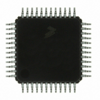
MC9S08DZ60ACLF Freescale Semiconductor, MC9S08DZ60ACLF Datasheet - Page 381

MC9S08DZ60ACLF
Manufacturer Part Number
MC9S08DZ60ACLF
Description
IC MCU 60K FLASH 4K RAM 48-LQFP
Manufacturer
Freescale Semiconductor
Series
HCS08r
Datasheets
1.DEMO9S08DZ60.pdf
(416 pages)
2.EVB9S08DZ60.pdf
(4 pages)
3.MC9S08DZ48AMLF.pdf
(458 pages)
Specifications of MC9S08DZ60ACLF
Core Processor
HCS08
Core Size
8-Bit
Speed
40MHz
Connectivity
CAN, I²C, LIN, SCI, SPI
Peripherals
LVD, POR, PWM, WDT
Number Of I /o
39
Program Memory Size
60KB (60K x 8)
Program Memory Type
FLASH
Eeprom Size
2K x 8
Ram Size
4K x 8
Voltage - Supply (vcc/vdd)
2.7 V ~ 5.5 V
Data Converters
A/D 16x12b
Oscillator Type
External
Operating Temperature
-40°C ~ 85°C
Package / Case
48-LQFP
Processor Series
S08DZ
Core
HCS08
Data Bus Width
8 bit
Data Ram Size
4 KB
Interface Type
CAN, I2C, SCI, SPI
Maximum Clock Frequency
40 MHz
Number Of Programmable I/os
53
Number Of Timers
2
Operating Supply Voltage
5.5 V
Maximum Operating Temperature
+ 85 C
Mounting Style
SMD/SMT
3rd Party Development Tools
EWS08
Development Tools By Supplier
DEMO9S08DZ60
Minimum Operating Temperature
- 40 C
On-chip Adc
12 bit, 24 Channel
For Use With
DEMO9S08DZ60 - BOARD DEMOEVB9S08DZ60 - BOARD EVAL FOR 9S08DZ60
Lead Free Status / RoHS Status
Lead free / RoHS Compliant
Available stocks
Company
Part Number
Manufacturer
Quantity
Price
Company:
Part Number:
MC9S08DZ60ACLF
Manufacturer:
FREESCAL
Quantity:
1 250
Company:
Part Number:
MC9S08DZ60ACLF
Manufacturer:
Freescale Semiconductor
Quantity:
10 000
- Current page: 381 of 458
- Download datasheet (5Mb)
17.2.1
BKGD is the single-wire background debug interface pin. The primary function of this pin is for
bidirectional serial communication of active background mode commands and data. During reset, this pin
is used to select between starting in active background mode or starting the user’s application program.
This pin is also used to request a timed sync response pulse to allow a host development tool to determine
the correct clock frequency for background debug serial communications.
BDC serial communications use a custom serial protocol first introduced on the M68HC12 Family of
microcontrollers. This protocol assumes the host knows the communication clock rate that is determined
by the target BDC clock rate. All communication is initiated and controlled by the host that drives a
high-to-low edge to signal the beginning of each bit time. Commands and data are sent most significant bit
first (MSB first). For a detailed description of the communications protocol, refer to
“Communication
If a host is attempting to communicate with a target MCU that has an unknown BDC clock rate, a SYNC
command may be sent to the target MCU to request a timed sync response signal from which the host can
determine the correct communication speed.
BKGD is a pseudo-open-drain pin and there is an on-chip pullup so no external pullup resistor is required.
Unlike typical open-drain pins, the external RC time constant on this pin, which is influenced by external
capacitance, plays almost no role in signal rise time. The custom protocol provides for brief, actively
driven speedup pulses to force rapid rise times on this pin without risking harmful drive level conflicts.
Refer to
When no debugger pod is connected to the 6-pin BDM interface connector, the internal pullup on BKGD
chooses normal operating mode. When a debug pod is connected to BKGD it is possible to force the MCU
into active background mode after reset. The specific conditions for forcing active background depend
upon the HCS08 derivative (refer to the introduction to this Development Support section). It is not
necessary to reset the target MCU to communicate with it through the background debug interface.
17.2.2
The BDC serial interface requires the external controller to generate a falling edge on the BKGD pin to
indicate the start of each bit time. The external controller provides this falling edge whether data is
transmitted or received.
BKGD is a pseudo-open-drain pin that can be driven either by an external controller or by the MCU. Data
is transferred MSB first at 16 BDC clock cycles per bit (nominal speed). The interface times out if
512 BDC clock cycles occur between falling edges from the host. Any BDC command that was in progress
Freescale Semiconductor
Section 17.2.2, “Communication
BKGD Pin Description
Communication Details
Details.”
MC9S08DZ128 Series Data Sheet, Rev. 1
Figure 17-1. BDM Tool Connector
NO CONNECT 3
NO CONNECT 5
Details,”
BKGD
1
for more detail.
2
4
6
GND
RESET
V
DD
Chapter 17 Development Support
Section 17.2.2,
381
Related parts for MC9S08DZ60ACLF
Image
Part Number
Description
Manufacturer
Datasheet
Request
R
Part Number:
Description:
Manufacturer:
Freescale Semiconductor, Inc
Datasheet:
Part Number:
Description:
Manufacturer:
Freescale Semiconductor, Inc
Datasheet:
Part Number:
Description:
Manufacturer:
Freescale Semiconductor, Inc
Datasheet:
Part Number:
Description:
Manufacturer:
Freescale Semiconductor, Inc
Datasheet:
Part Number:
Description:
Manufacturer:
Freescale Semiconductor, Inc
Datasheet:
Part Number:
Description:
Manufacturer:
Freescale Semiconductor, Inc
Datasheet:
Part Number:
Description:
Manufacturer:
Freescale Semiconductor, Inc
Datasheet:
Part Number:
Description:
Manufacturer:
Freescale Semiconductor, Inc
Datasheet:
Part Number:
Description:
Manufacturer:
Freescale Semiconductor, Inc
Datasheet:
Part Number:
Description:
Manufacturer:
Freescale Semiconductor, Inc
Datasheet:
Part Number:
Description:
Manufacturer:
Freescale Semiconductor, Inc
Datasheet:
Part Number:
Description:
Manufacturer:
Freescale Semiconductor, Inc
Datasheet:
Part Number:
Description:
Manufacturer:
Freescale Semiconductor, Inc
Datasheet:
Part Number:
Description:
Manufacturer:
Freescale Semiconductor, Inc
Datasheet:
Part Number:
Description:
Manufacturer:
Freescale Semiconductor, Inc
Datasheet:


