MC9S08DZ60ACLF Freescale Semiconductor, MC9S08DZ60ACLF Datasheet - Page 12
MC9S08DZ60ACLF
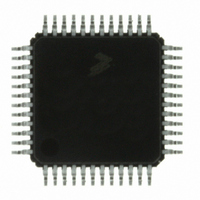
Manufacturer Part Number
MC9S08DZ60ACLF
Description
IC MCU 60K FLASH 4K RAM 48-LQFP
Manufacturer
Freescale Semiconductor
Series
HCS08r
Datasheets
1.DEMO9S08DZ60.pdf
(416 pages)
2.EVB9S08DZ60.pdf
(4 pages)
3.MC9S08DZ48AMLF.pdf
(458 pages)
Specifications of MC9S08DZ60ACLF
Core Processor
HCS08
Core Size
8-Bit
Speed
40MHz
Connectivity
CAN, I²C, LIN, SCI, SPI
Peripherals
LVD, POR, PWM, WDT
Number Of I /o
39
Program Memory Size
60KB (60K x 8)
Program Memory Type
FLASH
Eeprom Size
2K x 8
Ram Size
4K x 8
Voltage - Supply (vcc/vdd)
2.7 V ~ 5.5 V
Data Converters
A/D 16x12b
Oscillator Type
External
Operating Temperature
-40°C ~ 85°C
Package / Case
48-LQFP
Processor Series
S08DZ
Core
HCS08
Data Bus Width
8 bit
Data Ram Size
4 KB
Interface Type
CAN, I2C, SCI, SPI
Maximum Clock Frequency
40 MHz
Number Of Programmable I/os
53
Number Of Timers
2
Operating Supply Voltage
5.5 V
Maximum Operating Temperature
+ 85 C
Mounting Style
SMD/SMT
3rd Party Development Tools
EWS08
Development Tools By Supplier
DEMO9S08DZ60
Minimum Operating Temperature
- 40 C
On-chip Adc
12 bit, 24 Channel
For Use With
DEMO9S08DZ60 - BOARD DEMOEVB9S08DZ60 - BOARD EVAL FOR 9S08DZ60
Lead Free Status / RoHS Status
Lead free / RoHS Compliant
Available stocks
Company
Part Number
Manufacturer
Quantity
Price
Company:

Part Number:
MC9S08DZ60ACLF
Manufacturer:
FREESCAL
Quantity:
1 250
Company:
Part Number:
MC9S08DZ60ACLF
Manufacturer:
Freescale Semiconductor
Quantity:
10 000


Section Number
7.5
7.6
8.1
8.2
8.3
8.4
8.5
9.1
9.2
12
CALL and RTC Instructions ..........................................................................................................151
HCS08 Instruction Set Summary ...................................................................................................153
Introduction ....................................................................................................................................165
External Signal Description ...........................................................................................................169
Register Definition .........................................................................................................................170
Functional Description ...................................................................................................................178
Initialization / Application Information .........................................................................................185
Introduction ....................................................................................................................................199
External Signal Description ...........................................................................................................203
7.4.2 Interrupt Sequence ..........................................................................................................149
7.4.3 Wait Mode Operation ......................................................................................................150
7.4.4 Stop Mode Operation ......................................................................................................150
7.4.5 BGND Instruction ...........................................................................................................151
8.1.1 Features ...........................................................................................................................167
8.1.2 Modes of Operation ........................................................................................................169
8.3.1 MCG Control Register 1 (MCGC1) ...............................................................................170
8.3.2 MCG Control Register 2 (MCGC2) ...............................................................................172
8.3.3 MCG Trim Register (MCGTRM) ...................................................................................173
8.3.4 MCG Status and Control Register (MCGSC) .................................................................174
8.3.5 MCG Control Register 3 (MCGC3) ...............................................................................175
8.3.6 MCG Test and Control Register (MCGT) ......................................................................177
8.4.1 Operational Modes ..........................................................................................................178
8.4.2 Mode Switching ..............................................................................................................182
8.4.3 Bus Frequency Divider ...................................................................................................183
8.4.4 Low Power Bit Usage .....................................................................................................183
8.4.5 Internal Reference Clock ................................................................................................183
8.4.6 External Reference Clock ...............................................................................................183
8.4.7 Fixed Frequency Clock ...................................................................................................184
8.5.1 MCG Module Initialization Sequence ............................................................................185
8.5.2 Using a 32.768 kHz Reference .......................................................................................186
8.5.3 MCG Mode Switching ....................................................................................................187
8.5.4 Calibrating the Internal Reference Clock (IRC) .............................................................195
9.1.1 ACMP Configuration Information ..................................................................................199
9.1.2 Features ...........................................................................................................................201
9.1.3 Modes of Operation ........................................................................................................201
9.1.4 Block Diagram ................................................................................................................201
Multi-Purpose Clock Generator (S08MCGV2)
5-V Analog Comparator (S08ACMPV3)
MC9S08DZ128 Series Data Sheet, Rev. 1
Chapter 8
Chapter 9
Title
Freescale Semiconductor
Page
Related parts for MC9S08DZ60ACLF
Image
Part Number
Description
Manufacturer
Datasheet
Request
R

Part Number:
Description:
Manufacturer:
Freescale Semiconductor, Inc
Datasheet:
Part Number:
Description:
Manufacturer:
Freescale Semiconductor, Inc
Datasheet:
Part Number:
Description:
Manufacturer:
Freescale Semiconductor, Inc
Datasheet:
Part Number:
Description:
Manufacturer:
Freescale Semiconductor, Inc
Datasheet:
Part Number:
Description:
Manufacturer:
Freescale Semiconductor, Inc
Datasheet:
Part Number:
Description:
Manufacturer:
Freescale Semiconductor, Inc
Datasheet:
Part Number:
Description:
Manufacturer:
Freescale Semiconductor, Inc
Datasheet:
Part Number:
Description:
Manufacturer:
Freescale Semiconductor, Inc
Datasheet:
Part Number:
Description:
Manufacturer:
Freescale Semiconductor, Inc
Datasheet:
Part Number:
Description:
Manufacturer:
Freescale Semiconductor, Inc
Datasheet:
Part Number:
Description:
Manufacturer:
Freescale Semiconductor, Inc
Datasheet:
Part Number:
Description:
Manufacturer:
Freescale Semiconductor, Inc
Datasheet:
Part Number:
Description:
Manufacturer:
Freescale Semiconductor, Inc
Datasheet:
Part Number:
Description:
Manufacturer:
Freescale Semiconductor, Inc
Datasheet:
Part Number:
Description:
Manufacturer:
Freescale Semiconductor, Inc
Datasheet: