MC908GR60ACFAE Freescale Semiconductor, MC908GR60ACFAE Datasheet - Page 27
MC908GR60ACFAE
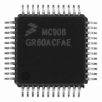
Manufacturer Part Number
MC908GR60ACFAE
Description
IC MCU 60K FLASH 8MHZ 48-LQFP
Manufacturer
Freescale Semiconductor
Series
HC08r
Datasheet
1.MC908GR32ACFJE.pdf
(314 pages)
Specifications of MC908GR60ACFAE
Core Processor
HC08
Core Size
8-Bit
Speed
8MHz
Connectivity
SCI, SPI
Peripherals
LVD, POR, PWM
Number Of I /o
37
Program Memory Size
60KB (60K x 8)
Program Memory Type
FLASH
Ram Size
2K x 8
Voltage - Supply (vcc/vdd)
3 V ~ 5.5 V
Data Converters
A/D 24x10b
Oscillator Type
Internal
Operating Temperature
-40°C ~ 85°C
Package / Case
48-LQFP
Controller Family/series
HC08
No. Of I/o's
37
Ram Memory Size
2KB
Cpu Speed
8MHz
No. Of Timers
2
Embedded Interface Type
SCI, SPI
Rohs Compliant
Yes
Processor Series
HC08GR
Core
HC08
Data Bus Width
8 bit
Data Ram Size
2 KB
Interface Type
ESCI, SPI
Maximum Clock Frequency
8 MHz
Number Of Programmable I/os
53
Number Of Timers
8
Maximum Operating Temperature
+ 85 C
Mounting Style
SMD/SMT
Development Tools By Supplier
FSICEBASE, DEMO908GZ60E, M68CBL05CE, M68EML08GPGTE
Minimum Operating Temperature
- 40 C
On-chip Adc
10 bit, 24 Channel
Lead Free Status / RoHS Status
Lead free / RoHS Compliant
Eeprom Size
-
Lead Free Status / Rohs Status
Details
Available stocks
Company
Part Number
Manufacturer
Quantity
Price
Company:

Part Number:
MC908GR60ACFAE
Manufacturer:
Freescale Semiconductor
Quantity:
10 000
Part Number:
MC908GR60ACFAE
Manufacturer:
FREESCALE
Quantity:
20 000


V
to the same voltage potential as V
1.5.8 Port A Input/Output (I/O) Pins (PTA7/KBD7/AD15–PTA0/KBD0/AD8)
PTA7–PTA0 are general-purpose, bidirectional I/O port pins. Any or all of the port A pins can be
programmed to serve as keyboard interrupt pins or used as analog-to-digital inputs. PTA7–PTA4 are only
available on the 48-pin LQFP and 64-pin QFP packages. See
Chapter 9 Keyboard Interrupt Module
These port pins also have selectable pullups when configured for input mode. The pullups are disengaged
when configured for output mode. The pullups are selectable on an individual port bit basis.
1.5.9 Port B I/O Pins (PTB7/AD7–PTB0/AD0)
PTB7–PTB0 are general-purpose, bidirectional I/O port pins that can also be used for analog-to-digital
converter (ADC) inputs. PTB7–PTB6 are only available on the 48-pin LQFP and 64-pin QFP packages.
See
1.5.10 Port C I/O Pins (PTC6–PTC0)
PTC6 and PTC5 are general-purpose, bidirectional I/O port pins.
PTC4–PTC0 are general-purpose, bidirectional I/O port pins that contain higher current sink/source
capability. PTC6–PTC2 are only available on the 48-pin LQFP and 64-pin QFP packages. See
12 Input/Output (I/O)
These port pins also have selectable pullups when configured for input mode. The pullups are disengaged
when configured for output mode. The pullups are selectable on an individual port bit basis.
1.5.11 Port D I/O Pins (PTD7/T2CH1–PTD0/SS)
PTD7–PTD0 are special-function, bidirectional I/O port pins. PTD3–PTD0 can be programmed to be
serial peripheral interface (SPI) pins, while PTD7–PTD4 can be individually programmed to be timer
interface module (TIM1 and TIM2) pins. PTD0 can be used to output a clock, MCLK. PTD7 is only
available on the 48-pin LQFP and 64-pin QFP packages. See
Chapter 18 Timer Interface Module
12 Input/Output (I/O)
These port pins also have selectable pullups when configured for input mode. The pullups are disengaged
when configured for output mode. The pullups are selectable on an individual port bit basis.
1.5.12 Port E I/O Pins (PTE5–PTE2, PTE1/RxD, and PTE0/TxD)
PTE5–PTE0 are general-purpose, bidirectional I/O port pins. PTE1 and PTE0 can also be programmed
to be enhanced serial communications interface (ESCI) pins. PTE5–PTE2 are only available on the
48-pin LQFP and 64-pin QFP packages. See
(ESCI) Module
1.5.13 Port F I/O Pins (PTF7/T2CH5–PTF0)
PTF7–PTF4 are special-function, bidirectional I/O port pins that can be individually programmed to be
timer interface module (TIM2) pins.
Freescale Semiconductor
REFL
Chapter 12 Input/Output (I/O) Ports
is the low reference supply for the ADC, and by default the V
and
MC68HC908GR60A • MC68HC908GR48A • MC68HC908GR32A Data Sheet, Rev. 5
Chapter 12 Input/Output (I/O)
Ports.
Ports, and
Chapter 5 Configuration Register
SS
(TIM2),
. See
(KBI), and
and
Chapter 3 Analog-to-Digital Converter
Chapter 15 Serial Peripheral Interface (SPI)
Chapter 3 Analog-to-Digital Converter
Chapter 13 Enhanced Serial Communications Interface
Chapter 3 Analog-to-Digital Converter
Ports.
Chapter 17 Timer Interface Module
Chapter 12 Input/Output (I/O)
(CONFIG).
SSAD
/V
REFL
pin should be connected
(ADC).
(ADC).
Module,
(ADC).
Pin Functions
Ports,
Chapter
Chapter
(TIM1),
27
Related parts for MC908GR60ACFAE
Image
Part Number
Description
Manufacturer
Datasheet
Request
R

Part Number:
Description:
Manufacturer:
Freescale Semiconductor, Inc
Datasheet:
Part Number:
Description:
Manufacturer:
Freescale Semiconductor, Inc
Datasheet:
Part Number:
Description:
Manufacturer:
Freescale Semiconductor, Inc
Datasheet:
Part Number:
Description:
Manufacturer:
Freescale Semiconductor, Inc
Datasheet:
Part Number:
Description:
Manufacturer:
Freescale Semiconductor, Inc
Datasheet:
Part Number:
Description:
Manufacturer:
Freescale Semiconductor, Inc
Datasheet:
Part Number:
Description:
Manufacturer:
Freescale Semiconductor, Inc
Datasheet:
Part Number:
Description:
Manufacturer:
Freescale Semiconductor, Inc
Datasheet:
Part Number:
Description:
Manufacturer:
Freescale Semiconductor, Inc
Datasheet:
Part Number:
Description:
Manufacturer:
Freescale Semiconductor, Inc
Datasheet:
Part Number:
Description:
Manufacturer:
Freescale Semiconductor, Inc
Datasheet:
Part Number:
Description:
Manufacturer:
Freescale Semiconductor, Inc
Datasheet:
Part Number:
Description:
Manufacturer:
Freescale Semiconductor, Inc
Datasheet:
Part Number:
Description:
Manufacturer:
Freescale Semiconductor, Inc
Datasheet:
Part Number:
Description:
Manufacturer:
Freescale Semiconductor, Inc
Datasheet: