MC9S12C128CFUE Freescale Semiconductor, MC9S12C128CFUE Datasheet - Page 512
MC9S12C128CFUE
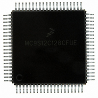
Manufacturer Part Number
MC9S12C128CFUE
Description
IC MCU 128K FLASH 25MHZ 80-QFP
Manufacturer
Freescale Semiconductor
Series
HCS12r
Specifications of MC9S12C128CFUE
Core Processor
HCS12
Core Size
16-Bit
Speed
25MHz
Connectivity
CAN, EBI/EMI, SCI, SPI
Peripherals
POR, PWM, WDT
Number Of I /o
60
Program Memory Size
128KB (128K x 8)
Program Memory Type
FLASH
Ram Size
4K x 8
Voltage - Supply (vcc/vdd)
2.35 V ~ 5.5 V
Data Converters
A/D 8x10b
Oscillator Type
Internal
Operating Temperature
-40°C ~ 85°C
Package / Case
80-QFP
Cpu Family
HCS12
Device Core Size
16b
Frequency (max)
25MHz
Interface Type
CAN/SCI/SPI
Total Internal Ram Size
4KB
# I/os (max)
60
Number Of Timers - General Purpose
8
Operating Supply Voltage (typ)
2.5/5V
Operating Supply Voltage (max)
2.75/5.5V
Operating Supply Voltage (min)
2.35/2.97V
On-chip Adc
8-chx10-bit
Instruction Set Architecture
CISC
Operating Temp Range
-40C to 85C
Operating Temperature Classification
Industrial
Mounting
Surface Mount
Pin Count
80
Package Type
PQFP
Processor Series
S12C
Core
HCS12
Data Bus Width
16 bit
Data Ram Size
4000 B
Maximum Clock Frequency
25 MHz
Number Of Programmable I/os
61
Number Of Timers
1
Operating Supply Voltage
- 0.3 V to + 6.5 V
Maximum Operating Temperature
+ 85 C
Mounting Style
SMD/SMT
3rd Party Development Tools
EWHCS12
Development Tools By Supplier
M68EVB912C32EE
Minimum Operating Temperature
- 40 C
Lead Free Status / RoHS Status
Lead free / RoHS Compliant
Eeprom Size
-
Lead Free Status / Rohs Status
Compliant
Available stocks
Company
Part Number
Manufacturer
Quantity
Price
Company:

Part Number:
MC9S12C128CFUE
Manufacturer:
ST
Quantity:
6 246
Company:
Part Number:
MC9S12C128CFUE
Manufacturer:
Freescale Semiconductor
Quantity:
10 000


Chapter 18 32 Kbyte Flash Module (S12FTS32KV1)
FPHDIS is cleared. The FPROT register is loaded from Flash address 0xFF0D during the reset sequence,
indicated by F in
To change the Flash protection that will be loaded on reset, the upper sector of the Flash array must be
unprotected, then the Flash protection byte located at Flash address 0xFF0D must be written to.
A protected Flash sector is disabled by FPHDIS
defined by FPHS[1:0]
Trying to alter any of the protected areas will result in a protect violation error and the PVIOL flag will be
set in the FSTAT register (see
when protection is fully disabled by setting the
erase a Flash array while protection is enabled will set the PVIOL flag in the FSTAT register.
512
FPHS[1:0]
FPLS[1:0]
FPOPEN
FPHDIS
FPLDIS
Field
NV6
4–3
1–0
7
6
5
2
Protection Function for Program or Erase — It is possible using the FPOPEN bit to either select address
ranges to be protected using FPHDIS, FPLDIS, FPHS[1:0] and FPLS[1:0] or to select the same ranges to be
unprotected. When FPOPEN is set, FPxDIS enables the ranges to be protected, whereby clearing FPxDIS
enables protection for the range specified by the corresponding FPxS[1:0] bits. When FPOPEN is cleared,
FPxDIS defines unprotected ranges as specified by the corresponding FPxS[1:0] bits. In this case, setting
FPxDIS enables protection. Thus the effective polarity of the FPxDIS bits is swapped by the FPOPEN bit as
shown in
can remain unprotected for EEPROM emulation.
0 The FPHDIS and FPLDIS bits define Flash address ranges to be unprotected
1 The FPHDIS and FPLDIS bits define Flash address ranges to be protected
Nonvolatile Flag Bit — The NV6 bit should remain in the erased state for future enhancements.
Flash Protection Higher Address Range Disable — The FPHDIS bit determines whether there is a
protected/unprotected area in the higher space of the Flash address map.
0 Protection/unprotection enabled
1 Protection/unprotection disabled
Flash Protection Higher Address Size — The FPHS[1:0] bits determine the size of the protected/unprotected
sector as shown in
Flash Protection Lower Address Range Disable — The FPLDIS bit determines whether there is a
protected/unprotected sector in the lower space of the Flash address map.
0 Protection/unprotection enabled
1 Protection/unprotection disabled
Flash Protection Lower Address Size — The FPLS[1:0] bits determine the size of the protected/unprotected
sector as shown in
Figure
Table
and FPLS[1:0]
18-8.
18-9. This function allows the main part of the Flash array to be protected while a small range
Table
Table
Section
18-10. The FPHS[1:0] bits can only be written to while the FPHDIS bit is set.
18-11. The FPLS[1:0] bits can only be written to while the FPLDIS bit is set.
Table 18-8. FPROT Field Descriptions
MC9S12C-Family / MC9S12GC-Family
in the FPROT register.
18.3.2.6). A mass erase of the whole Flash array is only possible
FPOPEN, FPLDIS,
Rev 01.24
and FPLDIS
Description
while the size of the protected sector is
and FPHDIS bits. An attempt to mass
Freescale Semiconductor
Related parts for MC9S12C128CFUE
Image
Part Number
Description
Manufacturer
Datasheet
Request
R

Part Number:
Description:
Manufacturer:
Freescale Semiconductor, Inc
Datasheet:
Part Number:
Description:
Manufacturer:
Freescale Semiconductor, Inc
Datasheet:
Part Number:
Description:
Manufacturer:
Freescale Semiconductor, Inc
Datasheet:
Part Number:
Description:
Manufacturer:
Freescale Semiconductor, Inc
Datasheet:
Part Number:
Description:
Manufacturer:
Freescale Semiconductor, Inc
Datasheet:
Part Number:
Description:
Manufacturer:
Freescale Semiconductor, Inc
Datasheet:
Part Number:
Description:
Manufacturer:
Freescale Semiconductor, Inc
Datasheet:
Part Number:
Description:
Manufacturer:
Freescale Semiconductor, Inc
Datasheet:
Part Number:
Description:
Manufacturer:
Freescale Semiconductor, Inc
Datasheet:
Part Number:
Description:
Manufacturer:
Freescale Semiconductor, Inc
Datasheet:
Part Number:
Description:
Manufacturer:
Freescale Semiconductor, Inc
Datasheet:
Part Number:
Description:
Manufacturer:
Freescale Semiconductor, Inc
Datasheet:
Part Number:
Description:
Manufacturer:
Freescale Semiconductor, Inc
Datasheet:
Part Number:
Description:
Manufacturer:
Freescale Semiconductor, Inc
Datasheet:
Part Number:
Description:
Manufacturer:
Freescale Semiconductor, Inc
Datasheet: