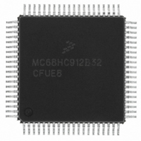
MCHC912B32CFUE8 Freescale Semiconductor, MCHC912B32CFUE8 Datasheet - Page 137

MCHC912B32CFUE8
Manufacturer Part Number
MCHC912B32CFUE8
Description
IC MCU 32K FLASH 8MHZ 80-QFP
Manufacturer
Freescale Semiconductor
Series
HC12r
Datasheet
1.MCHC912B32CFUE8.pdf
(334 pages)
Specifications of MCHC912B32CFUE8
Core Processor
CPU12
Core Size
16-Bit
Speed
8MHz
Connectivity
SCI, SPI
Peripherals
POR, PWM, WDT
Number Of I /o
63
Program Memory Size
32KB (32K x 8)
Program Memory Type
FLASH
Eeprom Size
768 x 8
Ram Size
1K x 8
Voltage - Supply (vcc/vdd)
4.5 V ~ 5.5 V
Data Converters
A/D 8x10b
Oscillator Type
External
Operating Temperature
-40°C ~ 85°C
Package / Case
80-QFP
Cpu Family
HC12
Device Core Size
16b
Frequency (max)
8MHz
Interface Type
SCI/SPI
Total Internal Ram Size
1KB
# I/os (max)
63
Operating Supply Voltage (typ)
5V
Operating Supply Voltage (max)
5.5V
Operating Supply Voltage (min)
4.5V
On-chip Adc
8-chx10-bit
Instruction Set Architecture
CISC
Operating Temp Range
-40C to 85C
Operating Temperature Classification
Industrial
Mounting
Surface Mount
Pin Count
80
Package Type
PQFP
Package
80PQFP
Family Name
HC12
Maximum Speed
8 MHz
Operating Supply Voltage
5 V
Data Bus Width
16 Bit
Number Of Programmable I/os
63
Processor Series
HC912B
Core
HC12
Data Ram Size
1 KB
Maximum Clock Frequency
8 MHz
Maximum Operating Temperature
+ 85 C
Mounting Style
SMD/SMT
3rd Party Development Tools
EWHCS12
Development Tools By Supplier
M68EVB912B32E
Minimum Operating Temperature
- 40 C
Lead Free Status / RoHS Status
Lead free / RoHS Compliant
Available stocks
Company
Part Number
Manufacturer
Quantity
Price
Company:
Part Number:
MCHC912B32CFUE8
Manufacturer:
Freescale Semiconductor
Quantity:
10 000
- Current page: 137 of 334
- Download datasheet (2Mb)
11.2.13 PWM Special Mode Register
Read: Anytime
Write: Only in special mode (SMODN = 0)
These bits are available only in special mode and are reset in normal mode.
DISCR — Disable Channel Counter Reset Bit
DISCP — Disable Compare Count Period Bit
DISCAL — Disable Scale Counter Loading Bit
11.2.14 Port P Data Register
Read: Anytime
Write: Anytime
PWM functions share port P pins 3 to 0 and take precedence over the general-purpose port when
enabled. When configured as input, a read returns the pin level. When configured as output, a read
returns the latched output data.
A write drives associated pins only if configured for output and the corresponding PWM channel is not
enabled. After reset, all pins are general-purpose, high-impedance inputs.
Freescale Semiconductor
This bit disables the normal operation of resetting the channel counter when the channel counter is
written.
This bit disables the normal operation of loading scale counters on a write to the associated scale
register.
0 = Normal operation
1 = Write to PWM channel counter does not reset channel counter.
0 = Normal operation
1 = In left-aligned output mode, match of the period does not reset the associated PWM counter
0 = Normal operation
1 = Write to PWSCAL0 and PWSCAL1 does not load scale counters.
register.
Address: $0055
Address: $0056
Reset:
Reset:
Read:
Read:
Write:
Write:
PWM
DISCR
Bit 7
Bit 7
PP7
Figure 11-25. PWM Special Mode Register (PWTST)
0
Figure 11-26. Port P Data Register (PORTP)
DISCP
= Unimplemented
PP6
6
0
6
M68HC12B Family Data Sheet, Rev. 9.1
DISCAL
PP5
5
0
5
Unaffected by reset
PP4
4
0
0
4
PWM3
PP3
3
0
0
3
PWM2
PP2
2
0
0
2
PWM1
PP1
1
0
0
1
PWM Register Descriptions
PWM0
Bit 0
Bit 0
PP0
0
0
137
Related parts for MCHC912B32CFUE8
Image
Part Number
Description
Manufacturer
Datasheet
Request
R
Part Number:
Description:
Manufacturer:
Freescale Semiconductor, Inc
Datasheet:
Part Number:
Description:
Manufacturer:
Freescale Semiconductor, Inc
Datasheet:
Part Number:
Description:
Manufacturer:
Freescale Semiconductor, Inc
Datasheet:
Part Number:
Description:
Manufacturer:
Freescale Semiconductor, Inc
Datasheet:
Part Number:
Description:
Manufacturer:
Freescale Semiconductor, Inc
Datasheet:
Part Number:
Description:
Manufacturer:
Freescale Semiconductor, Inc
Datasheet:
Part Number:
Description:
Manufacturer:
Freescale Semiconductor, Inc
Datasheet:
Part Number:
Description:
Manufacturer:
Freescale Semiconductor, Inc
Datasheet:
Part Number:
Description:
Manufacturer:
Freescale Semiconductor, Inc
Datasheet:
Part Number:
Description:
Manufacturer:
Freescale Semiconductor, Inc
Datasheet:
Part Number:
Description:
Manufacturer:
Freescale Semiconductor, Inc
Datasheet:
Part Number:
Description:
Manufacturer:
Freescale Semiconductor, Inc
Datasheet:
Part Number:
Description:
Manufacturer:
Freescale Semiconductor, Inc
Datasheet:
Part Number:
Description:
Manufacturer:
Freescale Semiconductor, Inc
Datasheet:
Part Number:
Description:
Manufacturer:
Freescale Semiconductor, Inc
Datasheet:


