MCHC912B32CFUE8 Freescale Semiconductor, MCHC912B32CFUE8 Datasheet - Page 238
MCHC912B32CFUE8
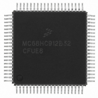
Manufacturer Part Number
MCHC912B32CFUE8
Description
IC MCU 32K FLASH 8MHZ 80-QFP
Manufacturer
Freescale Semiconductor
Series
HC12r
Datasheet
1.MCHC912B32CFUE8.pdf
(334 pages)
Specifications of MCHC912B32CFUE8
Core Processor
CPU12
Core Size
16-Bit
Speed
8MHz
Connectivity
SCI, SPI
Peripherals
POR, PWM, WDT
Number Of I /o
63
Program Memory Size
32KB (32K x 8)
Program Memory Type
FLASH
Eeprom Size
768 x 8
Ram Size
1K x 8
Voltage - Supply (vcc/vdd)
4.5 V ~ 5.5 V
Data Converters
A/D 8x10b
Oscillator Type
External
Operating Temperature
-40°C ~ 85°C
Package / Case
80-QFP
Cpu Family
HC12
Device Core Size
16b
Frequency (max)
8MHz
Interface Type
SCI/SPI
Total Internal Ram Size
1KB
# I/os (max)
63
Operating Supply Voltage (typ)
5V
Operating Supply Voltage (max)
5.5V
Operating Supply Voltage (min)
4.5V
On-chip Adc
8-chx10-bit
Instruction Set Architecture
CISC
Operating Temp Range
-40C to 85C
Operating Temperature Classification
Industrial
Mounting
Surface Mount
Pin Count
80
Package Type
PQFP
Package
80PQFP
Family Name
HC12
Maximum Speed
8 MHz
Operating Supply Voltage
5 V
Data Bus Width
16 Bit
Number Of Programmable I/os
63
Processor Series
HC912B
Core
HC12
Data Ram Size
1 KB
Maximum Clock Frequency
8 MHz
Maximum Operating Temperature
+ 85 C
Mounting Style
SMD/SMT
3rd Party Development Tools
EWHCS12
Development Tools By Supplier
M68EVB912B32E
Minimum Operating Temperature
- 40 C
Lead Free Status / RoHS Status
Lead free / RoHS Compliant
Available stocks
Company
Part Number
Manufacturer
Quantity
Price
Company:

Part Number:
MCHC912B32CFUE8
Manufacturer:
Freescale Semiconductor
Quantity:
10 000


Byte Data Link Communications (BDLC)
238
Bits I0, I1, I2, and I3 are cleared by a read of the BSVR register except when the BDLC data register
needs servicing (RDRF, RXIFR, or TDRE conditions). RXIFR and RDRF can only be cleared by a read
of the BSVR register followed by a read of BDR. TDRE can either be cleared by a read of the BSVR
register followed by a write to the BDLC BDR register, or by setting the TEOD bit in BCR2. Clearing
an invalid symbol flag requires an EOF flag to be received before the BDLC can receive or transmit. If
ALOOP or DLOOP in BCR2 is set, the BDLC node is disengaged from the J1850 bus. Therefore, the
BDLC does not receive any data from the J1850 bus which normally generates BSVR flags.
Upon receiving a BDLC interrupt, the user may read the value within the BSVR, transferring it to the
CPU’s index register. The value can be used to index a jump table to access a service routine. For
example:
SERVICE LDX
*
*
JMPTAB JMP
BSVR
$0C
$1C
$00
$04
$08
$10
$14
$18
$20
NOP instructions are used only to align the JMP instructions onto 4-byte
boundaries so that the value in the BSVR can be used intact. Each of the
service routines must end with an RTI instruction to guarantee correct
continued operation of the device. The first entry can be omitted since it
does not correspond to an interrupt.
JMP
NOP
JMP
NOP
JMP
NOP
.
.
.
JMP
END
I3
0
0
0
0
0
0
0
0
1
I2
0
0
0
0
1
1
1
1
0
BSVR
JMPTAB,XEnter service routine,
SERVE0Service condition #0
SERVE1Service condition #1
SERVE2Service condition #2
SERVE8Service condition #8
I1
0
0
1
1
0
0
1
1
0
I0
1
0
1
0
1
0
1
0
0
M68HC12B Family Data Sheet, Rev. 9.1
Fetch State Vector Number
(must end in an RTI)
Table 15-4. Interrupt Sources
Cyclical redundancy check (CRC) error
BDLC Tx data register empty (TDRE)
BDLC Rx data register full (RDRF)
Symbol invalid or out of range
Received IFR byte (RXIFR)
NOTE
No interrupts pending
Loss of arbitration
Interrupt Source
Received EOF
Wakeup
Freescale Semiconductor
8 (highest)
Priority
(lowest)
0
1
2
3
4
5
6
7
Related parts for MCHC912B32CFUE8
Image
Part Number
Description
Manufacturer
Datasheet
Request
R

Part Number:
Description:
Manufacturer:
Freescale Semiconductor, Inc
Datasheet:
Part Number:
Description:
Manufacturer:
Freescale Semiconductor, Inc
Datasheet:
Part Number:
Description:
Manufacturer:
Freescale Semiconductor, Inc
Datasheet:
Part Number:
Description:
Manufacturer:
Freescale Semiconductor, Inc
Datasheet:
Part Number:
Description:
Manufacturer:
Freescale Semiconductor, Inc
Datasheet:
Part Number:
Description:
Manufacturer:
Freescale Semiconductor, Inc
Datasheet:
Part Number:
Description:
Manufacturer:
Freescale Semiconductor, Inc
Datasheet:
Part Number:
Description:
Manufacturer:
Freescale Semiconductor, Inc
Datasheet:
Part Number:
Description:
Manufacturer:
Freescale Semiconductor, Inc
Datasheet:
Part Number:
Description:
Manufacturer:
Freescale Semiconductor, Inc
Datasheet:
Part Number:
Description:
Manufacturer:
Freescale Semiconductor, Inc
Datasheet:
Part Number:
Description:
Manufacturer:
Freescale Semiconductor, Inc
Datasheet:
Part Number:
Description:
Manufacturer:
Freescale Semiconductor, Inc
Datasheet:
Part Number:
Description:
Manufacturer:
Freescale Semiconductor, Inc
Datasheet:
Part Number:
Description:
Manufacturer:
Freescale Semiconductor, Inc
Datasheet: