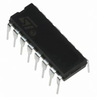
ST62T00CB6 STMicroelectronics, ST62T00CB6 Datasheet - Page 59

ST62T00CB6
Manufacturer Part Number
ST62T00CB6
Description
IC MCU 8BIT OTP 1K 16-PDIP
Manufacturer
STMicroelectronics
Series
ST6r
Specifications of ST62T00CB6
Core Processor
ST6
Core Size
8-Bit
Speed
8MHz
Peripherals
LVD, POR, WDT
Number Of I /o
9
Program Memory Size
1KB (1K x 8)
Program Memory Type
OTP
Ram Size
64 x 8
Voltage - Supply (vcc/vdd)
3 V ~ 6 V
Data Converters
A/D 4x8b
Oscillator Type
Internal
Operating Temperature
-40°C ~ 85°C
Package / Case
16-DIP (0.300", 7.62mm)
Controller Family/series
ST6
No. Of I/o's
9
Ram Memory Size
64Byte
Cpu Speed
8MHz
No. Of Timers
1
Rohs Compliant
Yes
Processor Series
ST62T0x
Core
ST6
Data Bus Width
8 bit
Data Ram Size
64 B
Maximum Clock Frequency
8 MHz
Number Of Programmable I/os
9
Number Of Timers
2
Operating Supply Voltage
3 V to 6 V
Maximum Operating Temperature
+ 85 C
Mounting Style
Through Hole
Development Tools By Supplier
ST622XC-KIT/110, ST62GP-EMU2, ST62E2XC-EPB/110, ST62E6XC-EPB/US, STREALIZER-II
Minimum Operating Temperature
- 40 C
On-chip Adc
8 bit
Cpu Family
ST6
Device Core Size
8b
Frequency (max)
8MHz
Total Internal Ram Size
64Byte
# I/os (max)
9
Number Of Timers - General Purpose
1
Operating Supply Voltage (typ)
3.3/5V
Operating Supply Voltage (max)
6V
Operating Supply Voltage (min)
3V
Instruction Set Architecture
CISC
Operating Temp Range
-40C to 85C
Operating Temperature Classification
Industrial
Mounting
Through Hole
Pin Count
16
Package Type
PDIP
Lead Free Status / RoHS Status
Lead free / RoHS Compliant
Eeprom Size
-
Connectivity
-
Lead Free Status / Rohs Status
In Transition
Other names
497-2093-5
Available stocks
Company
Part Number
Manufacturer
Quantity
Price
Company:
Part Number:
ST62T00CB6
Manufacturer:
MICRON
Quantity:
1 450
Company:
Part Number:
ST62T00CB6
Manufacturer:
STMicroelectronics
Quantity:
135
10.2 ABSOLUTE MAXIMUM RATINGS
Stresses above those listed as “absolute maxi-
mum ratings” may cause permanent damage to
the device. This is a stress rating only and func-
tional operation of the device under these condi-
10.2.1 Voltage Characteristics
10.2.2 Current Characteristics
10.2.3 Thermal Characteristics
Notes:
1. Directly connecting the RESET and I/O pins to V
2. When the current limitation is not possible, the V
3. Power (V
4. Negative injection disturbs the analog performance of the device. In particular, it induces leakage currents throughout
5. For ROM versions, it is forbidden to inject current on the NMI pin.
is generated or an unexpected change of the I/O configuration occurs (for example, due to a corrupted program coun-
ter). To guarantee safe operation, this connection has to be done through a pull-up or pull-down resistor (typical: 4.7k
for RESET, 10k for I/Os). Unused I/O pins must be tied in the same way to V
figuration.
I
the device including the analog inputs. To avoid undesirable effects on the analog functions, care must be taken:
- Analog input pins must have a negative injection less than 1mA (assuming that the impedance of the analog voltage
is lower than the specified limits).
- Pure digital pins must have a negative injection less than 1mA. In addition, it is recommended to inject the current as
far as possible from the analog input pins.
INJ(PIN)
I
INJ(PIN)
V
V
Symbol
Symbol
Symbol
ESD(HBM)
DD
V
T
I
I
specification. A positive injection is induced by V
V
VDD
VSS
I
OUT
STG
T
DD
IO
- V
IN
J
2) & 4)
) and ground (V
SS
Supply voltage
Input voltage on any pin
Output voltage on any pin
Electro-static discharge voltage (Human Body Model)
Total current into V
Total current out of V
Output current sunk by any standard I/O and control pin
Output current sunk by any high sink I/O pin
Output current source by any I/Os and control pin
Injected current on RESET pin
Injected current on any other pin
Storage temperature range
Maximum junction temperature
(see THERMAL CHARACTERISTICS
SS
) lines must always be connected to the external supply.
DD
SS
power lines (source)
Doc ID 4563 Rev 5
Ratings
Ratings
Ratings
ground lines (sink)
1) & 2)
DD
IN
1) & 2)
or V
absolute maximum rating must be respected, otherwise refer to
5)
SS
IN
>V
could damage the device if an unintentional internal reset
tions is not implied. Exposure to maximum rating
conditions for extended periods may affect device
reliability.
DD
section)
while a negative injection is induced by V
3)
3)
DD
ST6200C ST6201C ST6203C
or V
V
V
Maximum value
Maximum value
SS
SS
SS
-0.3 to V
-0.3 to V
-60 to +150
according to their reset con-
Value
3500
100
80
20
40
15
7
5
5
DD
DD
+0.3
+0.3
IN
<V
Unit
Unit
Unit
mA
°C
V
59/100
SS
.
1


