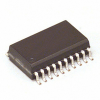
MC908JB16JDWE Freescale Semiconductor, MC908JB16JDWE Datasheet - Page 277

MC908JB16JDWE
Manufacturer Part Number
MC908JB16JDWE
Description
IC MCU 16K FLASH 6MHZ USB 20SOIC
Manufacturer
Freescale Semiconductor
Series
HC08r
Datasheets
1.MC908JB16DWE.pdf
(332 pages)
2.MC908JB12JDWE.pdf
(12 pages)
3.MC908JB16DWE.pdf
(332 pages)
Specifications of MC908JB16JDWE
Core Processor
HC08
Core Size
8-Bit
Speed
6MHz
Connectivity
SCI, USB
Peripherals
LED, LVD, POR, PWM
Number Of I /o
13
Program Memory Size
16KB (16K x 8)
Program Memory Type
FLASH
Ram Size
384 x 8
Voltage - Supply (vcc/vdd)
4 V ~ 5.5 V
Oscillator Type
Internal
Operating Temperature
0°C ~ 70°C
Package / Case
20-SOIC (7.5mm Width)
Processor Series
HC08JB
Core
HC08
Data Bus Width
8 bit
Data Ram Size
384 B
Interface Type
I2C/SCI/SPI/USB
Maximum Clock Frequency
32 MHz
Number Of Programmable I/os
21
Number Of Timers
4
Operating Supply Voltage
2.2 V
Maximum Operating Temperature
+ 70 C
Mounting Style
SMD/SMT
Development Tools By Supplier
FSICEBASE, DEMO908GZ60E, M68EML08GZE, KITUSBSPIDGLEVME, KITUSBSPIEVME, KIT33810EKEVME
Minimum Operating Temperature
0 C
Controller Family/series
HC08
No. Of I/o's
21
Ram Memory Size
384Byte
Cpu Speed
8MHz
No. Of Timers
2
Embedded Interface Type
SCI, USB
Rohs Compliant
Yes
Lead Free Status / RoHS Status
Lead free / RoHS Compliant
Eeprom Size
-
Data Converters
-
Lead Free Status / Rohs Status
Lead free / RoHS Compliant
Available stocks
Company
Part Number
Manufacturer
Quantity
Price
Company:
Part Number:
MC908JB16JDWE
Manufacturer:
FREESCALE
Quantity:
310
Company:
Part Number:
MC908JB16JDWE
Manufacturer:
Freescale Semiconductor
Quantity:
135
Part Number:
MC908JB16JDWE
Manufacturer:
FREESCALE
Quantity:
20 000
- Current page: 277 of 332
- Download datasheet (4Mb)
14.6.2 Data Direction Register E
MC68HC908JB16
Freescale Semiconductor
NOTE:
NOTE:
—
Rev. 1.1
Address:
Data direction register E (DDRE) does not affect the data direction of
port E pins that are being used by the TIM. However, the DDRE bits
always determine whether reading port E returns the states of the
latches or the states of the pins.
Data direction register E determines whether each port E pin is an input
or an output. Writing a logic 1 to a DDRE bit enables the output buffer for
the corresponding port E pin; a logic 0 disables the output buffer.
DDRE[4:0] — Data Direction Register E Bits
Avoid glitches on port E pins by writing to the port E data register before
changing data direction register E bits from 0 to 1.
Figure 14-13
Reset:
Read:
Write:
These read/write bits control port E data direction. Reset clears
DDRE[4:0], configuring all port E pins as inputs.
1 = Corresponding port E pin configured as output
0 = Corresponding port E pin configured as input
$0009
Bit 7
Figure 14-12. Data Direction Register E (DDRE)
0
0
shows the port E I/O circuit logic.
Input/Output (I/O) Ports
= Unimplemented
6
0
0
5
0
0
DDRE4
4
0
DDRE3
3
0
DDRE2
2
0
Input/Output (I/O) Ports
DDRE1
1
0
Technical Data
DDRE0
Bit 0
0
277
Related parts for MC908JB16JDWE
Image
Part Number
Description
Manufacturer
Datasheet
Request
R
Part Number:
Description:
Manufacturer:
Freescale Semiconductor, Inc
Datasheet:
Part Number:
Description:
Manufacturer:
Freescale Semiconductor, Inc
Datasheet:
Part Number:
Description:
Manufacturer:
Freescale Semiconductor, Inc
Datasheet:
Part Number:
Description:
Manufacturer:
Freescale Semiconductor, Inc
Datasheet:
Part Number:
Description:
Manufacturer:
Freescale Semiconductor, Inc
Datasheet:
Part Number:
Description:
Manufacturer:
Freescale Semiconductor, Inc
Datasheet:
Part Number:
Description:
Manufacturer:
Freescale Semiconductor, Inc
Datasheet:
Part Number:
Description:
Manufacturer:
Freescale Semiconductor, Inc
Datasheet:
Part Number:
Description:
Manufacturer:
Freescale Semiconductor, Inc
Datasheet:
Part Number:
Description:
Manufacturer:
Freescale Semiconductor, Inc
Datasheet:
Part Number:
Description:
Manufacturer:
Freescale Semiconductor, Inc
Datasheet:
Part Number:
Description:
Manufacturer:
Freescale Semiconductor, Inc
Datasheet:
Part Number:
Description:
Manufacturer:
Freescale Semiconductor, Inc
Datasheet:
Part Number:
Description:
Manufacturer:
Freescale Semiconductor, Inc
Datasheet:
Part Number:
Description:
Manufacturer:
Freescale Semiconductor, Inc
Datasheet:


