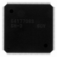
HD6417708SF60V Renesas Electronics America, HD6417708SF60V Datasheet - Page 124

HD6417708SF60V
Manufacturer Part Number
HD6417708SF60V
Description
IC SUPERH MPU ROMLESS 208LQFP
Manufacturer
Renesas Electronics America
Series
SuperH® SH7700r
Datasheet
1.HD6417708SF60V.pdf
(635 pages)
Specifications of HD6417708SF60V
Core Processor
SH-2
Core Size
32-Bit
Speed
60MHz
Connectivity
EBI/EMI, SCI, SmartCard
Peripherals
POR, WDT
Number Of I /o
8
Program Memory Type
ROMless
Voltage - Supply (vcc/vdd)
3 V ~ 3.6 V
Oscillator Type
External
Operating Temperature
-20°C ~ 75°C
Package / Case
208-LQFP
Lead Free Status / RoHS Status
Lead free / RoHS Compliant
Eeprom Size
-
Ram Size
-
Program Memory Size
-
Data Converters
-
Available stocks
Company
Part Number
Manufacturer
Quantity
Price
Company:
Part Number:
HD6417708SF60V
Manufacturer:
Renesas Electronics America
Quantity:
10 000
Part Number:
HD6417708SF60V
Manufacturer:
RENESAS/瑞萨
Quantity:
20 000
- Current page: 124 of 635
- Download datasheet (3Mb)
In the address field, specify the entry address for selecting the entry (bits 10–4), W for selecting
the way (bits 12–11: 00 is way 0, 01 is way 1, 10 is way 2, 11 is way 3 in normal mode (8-kbyte
cache); 00 and 10 are way 0, and 01 and 11 are way 1 in RAM mode), and H'F0 to indicate
address array access (bits 31–24).
When writing, specify bit 3 as the A bit. The A bit indicates whether addresses are compared
during writing. When the A bit is 1, the addresses of the four entries selected by the entry
addresses are compared to the addresses to be written into the address array specified in the data
field. Writing takes place to the way that has a hit. When a miss occurs, nothing is written to the
address array and no operation occurs. The way number (W) specified in bits 12–11 is not used.
When the A bit is 0, it is written to the entry selected with the entry address and way number
without comparing addresses. The address specified by bits 31–10 in the data specification in
figure 5.5 (1), address array access, is a virtual address. When the MMU is enabled, the address is
translated into a physical address, then the physical address is used in comparing addresses when
the A bit is 1. The physical address is written into the address array.
When reading, the address tag, V bit, U bit, and LRU bits of the entry specified by the entry
address and way number (W) are read using the data format shown in figure 5.5 without
comparing addresses. To invalidate a specific entry, specify the entry by its entry address and way
number, and write 0 to its V bit. To invalidate only an entry for an address to be invalidated,
specify 1 for the A bit.
When an entry for which 0 is written to the V bit has a U bit set to 1, if it is a valid entry it will be
written back. This allows coherency to be achieved between the external memory and cache by
invalidating the entry. However, when 0 is written to the V bit, 0 must also be written to the U bit
of that entry.
In the SH7708 Series, the top 3 bits of the 32-bit physical address are treated as a shadow (see
section 10, Bus State Controller (BSC)). Therefore, in the event of a cache miss, 0 is registered in
the top 3 bits of the address array address tag.
When directly changing the address array using the MOV instruction, also, a value other than 0
must not be set in the top 3 bits of the address tag.
5.4.2
Data Array
The data array is mapped onto H'F1000000 to H'F1FFFFFF. To access a data array, the 32-bit
address field (for read/write accesses) and 32-bit data field (for write accesses) must be specified.
The address field specifies information for selecting the entry to be accessed; the data field
specifies the longword data to be written to the data array (figure 5.5 (2)).
In the address field, specify the entry address for selecting the entry (bits 10–4), L for indicating
the longword position within the (16-byte) line (bits 3–2: 00 is longword 0, 01 is longword 1, 10 is
longword 2, 11 is longword 3), W for selecting the way (bits 12–11: 00 is way 0, 01 is way 1, 10
104
Related parts for HD6417708SF60V
Image
Part Number
Description
Manufacturer
Datasheet
Request
R

Part Number:
Description:
KIT STARTER FOR M16C/29
Manufacturer:
Renesas Electronics America
Datasheet:

Part Number:
Description:
KIT STARTER FOR R8C/2D
Manufacturer:
Renesas Electronics America
Datasheet:

Part Number:
Description:
R0K33062P STARTER KIT
Manufacturer:
Renesas Electronics America
Datasheet:

Part Number:
Description:
KIT STARTER FOR R8C/23 E8A
Manufacturer:
Renesas Electronics America
Datasheet:

Part Number:
Description:
KIT STARTER FOR R8C/25
Manufacturer:
Renesas Electronics America
Datasheet:

Part Number:
Description:
KIT STARTER H8S2456 SHARPE DSPLY
Manufacturer:
Renesas Electronics America
Datasheet:

Part Number:
Description:
KIT STARTER FOR R8C38C
Manufacturer:
Renesas Electronics America
Datasheet:

Part Number:
Description:
KIT STARTER FOR R8C35C
Manufacturer:
Renesas Electronics America
Datasheet:

Part Number:
Description:
KIT STARTER FOR R8CL3AC+LCD APPS
Manufacturer:
Renesas Electronics America
Datasheet:

Part Number:
Description:
KIT STARTER FOR RX610
Manufacturer:
Renesas Electronics America
Datasheet:

Part Number:
Description:
KIT STARTER FOR R32C/118
Manufacturer:
Renesas Electronics America
Datasheet:

Part Number:
Description:
KIT DEV RSK-R8C/26-29
Manufacturer:
Renesas Electronics America
Datasheet:

Part Number:
Description:
KIT STARTER FOR SH7124
Manufacturer:
Renesas Electronics America
Datasheet:

Part Number:
Description:
KIT STARTER FOR H8SX/1622
Manufacturer:
Renesas Electronics America
Datasheet:

Part Number:
Description:
KIT DEV FOR SH7203
Manufacturer:
Renesas Electronics America
Datasheet:


