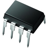
PIC12LCE673-04I/P Microchip Technology, PIC12LCE673-04I/P Datasheet - Page 100

PIC12LCE673-04I/P
Manufacturer Part Number
PIC12LCE673-04I/P
Description
IC MCU OTP 1KX14 LV A/D EE 8DIP
Manufacturer
Microchip Technology
Series
PIC® 12Cr
Specifications of PIC12LCE673-04I/P
Core Processor
PIC
Core Size
8-Bit
Speed
4MHz
Peripherals
POR, WDT
Number Of I /o
5
Program Memory Size
1.75KB (1K x 14)
Program Memory Type
OTP
Eeprom Size
16 x 8
Ram Size
128 x 8
Voltage - Supply (vcc/vdd)
2.5 V ~ 5.5 V
Data Converters
A/D 4x8b
Oscillator Type
Internal
Operating Temperature
-40°C ~ 85°C
Package / Case
8-DIP (0.300", 7.62mm)
Processor Series
PIC12LC
Core
PIC
Data Bus Width
8 bit
Data Ram Size
128 B
Maximum Clock Frequency
4 MHz
Number Of Programmable I/os
5
Number Of Timers
8
Operating Supply Voltage
2.5 V to 5.5 V
Maximum Operating Temperature
+ 85 C
Mounting Style
Through Hole
3rd Party Development Tools
52715-96, 52716-328, 52717-734
Development Tools By Supplier
ICE2000
Minimum Operating Temperature
- 40 C
On-chip Adc
8
Data Rom Size
128 B
Height
3.3 mm
Length
9.27 mm
Supply Voltage (max)
5.5 V
Supply Voltage (min)
2.5 V
Width
6.35 mm
Lead Free Status / RoHS Status
Lead free / RoHS Compliant
Connectivity
-
Lead Free Status / Rohs Status
Details
Available stocks
Company
Part Number
Manufacturer
Quantity
Price
Part Number:
PIC12LCE673-04I/P
Manufacturer:
MICROCHIP/微芯
Quantity:
20 000
PIC12C67X
12.6
FIGURE 12-5: EXTERNAL CLOCK TIMING
TABLE 12-1:
DS30561B-page 100
Note 1: Instruction cycle period (T
Parameter
CLKOUT
No.
1
2
3
4
OSC1
†
Timing Diagrams and Specifications
Data in "Typ" column is at 5V, 25°C unless otherwise stated. These parameters are for design guidance only and
are not tested.
on characterization data for that particular oscillator type under standard operating conditions with the device exe-
cuting code. Exceeding these specified limits may result in an unstable oscillator operation and/or higher than
expected current consumption. All devices are tested to operate at "min." values with an external clock applied to
the OSC1/CLKIN pin.
When an external clock input is used, the "Max." cycle time limit is "DC" (no clock) for all devices. OSC2 is discon-
nected (has no loading) for the PIC12C67X.
TosR,
TosL,
F
T
TosH
Sym
TosF
T
OSC
OSC
CY
CLOCK TIMING REQUIREMENTS
Characteristic
External CLKIN Frequency
(Note 1)
Oscillator Frequency
(Note 1)
External CLKIN Period
(Note 1)
Oscillator Period
(Note 1)
Instruction Cycle Time (Note 1) 400
External Clock in (OSC1) High
or Low Time
External Clock in (OSC1) Rise
or Fall Time
Q4
CY
) equals four times the input oscillator time-base period. All specified values are based
Q1
1
.455
Min
250
250
100
250
250
250
100
DC
DC
DC
DC
DC
2.5
50
10
—
—
—
Q2
4
4
5
5
5
Typ†
2
—
—
—
—
—
—
—
—
—
—
—
—
—
—
—
—
—
—
—
—
—
—
—
—
—
3
10,000
Q3
Max
200
200
250
250
DC
10
10
25
50
15
—
—
—
—
—
—
—
—
—
4
4
4
4
4
3
Units Conditions
MHz
MHz
MHz
MHz
MHz
MHz
MHz
kHz
kHz
ns
ns
ns
ns
ns
ns
ns
ns
ns
ns
ns
ns
ns
s
s
s
Q4
XT and EXTRC osc mode
HS osc mode (PIC12CE67X-04)
HS osc mode (PIC12CE67X-10)
LP osc mode
EXTRC osc mode
XT osc mode
HS osc mode (PIC12CE67X-04)
HS osc mode (PIC12CE67X-10)
LP osc mode
XT and EXTRC osc mode
HS osc mode (PIC12CE67X-04)
HS osc mode (PIC12CE67X-10)
LP osc mode
EXTRC osc mode
XT osc mode
HS osc mode (PIC12CE67X-04)
HS osc mode (PIC12CE67X-10)
LP osc mode
T
XT oscillator
LP oscillator
HS oscillator
XT oscillator
LP oscillator
HS oscillator
4
CY
= 4/F
1999 Microchip Technology Inc.
4
OSC
Q1


