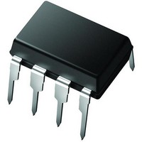
PIC12LCE673-04I/P Microchip Technology, PIC12LCE673-04I/P Datasheet - Page 61

PIC12LCE673-04I/P
Manufacturer Part Number
PIC12LCE673-04I/P
Description
IC MCU OTP 1KX14 LV A/D EE 8DIP
Manufacturer
Microchip Technology
Series
PIC® 12Cr
Specifications of PIC12LCE673-04I/P
Core Processor
PIC
Core Size
8-Bit
Speed
4MHz
Peripherals
POR, WDT
Number Of I /o
5
Program Memory Size
1.75KB (1K x 14)
Program Memory Type
OTP
Eeprom Size
16 x 8
Ram Size
128 x 8
Voltage - Supply (vcc/vdd)
2.5 V ~ 5.5 V
Data Converters
A/D 4x8b
Oscillator Type
Internal
Operating Temperature
-40°C ~ 85°C
Package / Case
8-DIP (0.300", 7.62mm)
Processor Series
PIC12LC
Core
PIC
Data Bus Width
8 bit
Data Ram Size
128 B
Maximum Clock Frequency
4 MHz
Number Of Programmable I/os
5
Number Of Timers
8
Operating Supply Voltage
2.5 V to 5.5 V
Maximum Operating Temperature
+ 85 C
Mounting Style
Through Hole
3rd Party Development Tools
52715-96, 52716-328, 52717-734
Development Tools By Supplier
ICE2000
Minimum Operating Temperature
- 40 C
On-chip Adc
8
Data Rom Size
128 B
Height
3.3 mm
Length
9.27 mm
Supply Voltage (max)
5.5 V
Supply Voltage (min)
2.5 V
Width
6.35 mm
Lead Free Status / RoHS Status
Lead free / RoHS Compliant
Connectivity
-
Lead Free Status / Rohs Status
Details
Available stocks
Company
Part Number
Manufacturer
Quantity
Price
Part Number:
PIC12LCE673-04I/P
Manufacturer:
MICROCHIP/微芯
Quantity:
20 000
FIGURE 9-10: EXTERNAL POWER-ON
Note 1: External Power-on Reset circuit is required only
1999 Microchip Technology Inc.
2: R < 40 k
3: R1 = 100
if V
helps discharge the capacitor quickly when V
powers down.
voltage drop across R does not violate the
device’s electrical specification.
into MCLR from external capacitor C, in the
event of MCLR/V
Electrostatic Discharge (ESD) or Electrical
Overstress (EOS).
D
DD
V
power-up slope is too slow. The diode D
DD
RESET CIRCUIT (FOR SLOW
V
R
DD
C
is recommended to make sure that
to 1 k
POWER-UP)
PP
R1
will limit any current flowing
pin breakdown due to
MCLR
PIC12C67X
DD
FIGURE 9-11: EXTERNAL BROWN-OUT
FIGURE 9-12: EXTERNAL BROWN-OUT
Note 1: This circuit will activate reset when V
Note 1: This brown-out circuit is less expensive,
V
V
2: Resistors should be adjusted for the character-
DD
DD
2: Resistors should be adjusted for the charac-
below (Vz + 0.7V), where Vz = Zener voltage.
istics of the transistor.
R1
R2
33k
albeit less accurate. Transistor Q1 turns off
when V
teristics of the transistor.
V
DD
PROTECTION CIRCUIT 1
PROTECTION CIRCUIT 2
DD
•
10k
is below a certain level such that:
R1 + R2
PIC12C67X
R1
Q1
4.3k
4.3k
= 0.7V
DS30561B-page 61
PIC12C67X
PIC12C67X
V
MCLR
V
MCLR
DD
DD
DD
goes


